In the electronics industry, “time to market” is everything. However, speed without a structured process leads to catastrophic field failures. A top-tier PCB supplier doesn’t just take your files and press “print.”
The journey from a digital Gerber file to a physical, high-reliability circuit board involves a synchronized dance between engineering, chemical processing, and rigorous quality gates within the PCB Factory. Here is the step-by-step workflow that ensures your project arrives on time and on spec.
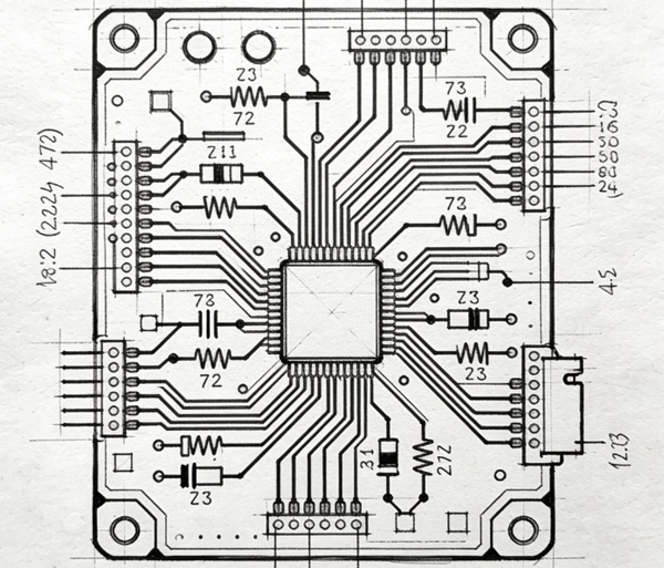
Phase 1: The Engineering “Gateway” (CAM & DFM)
The moment you place an order with your PCB supplier, the data enters the PCB factory’s CAM (Computer-Aided Manufacturing) department.
- DFM Check: Engineers scan for “acid traps,” insufficient annular rings, or clearance violations.
- Panelization: To optimize material usage and reduce costs, individual boards are arranged onto large production panels.
- Drill Data Generation: CNC paths are programmed for laser and mechanical drilling.
Phase 2: The Core Construction (Inner Layers & Lamination)
For multi-layer boards, the internal layers are processed first.
- Etching: Copper is removed from the core to create the inner-layer circuitry.
- Lamination: High-pressure vacuum presses bond the layers together using prepreg. A quality-focused PCB factory monitors temperature and pressure curves in real-time to prevent delamination.
Phase 3: Creating Connections (Drilling & Plating)
Once the “sandwich” is formed, holes are drilled to create vias.
- Electroless Copper: A thin layer of copper is chemically deposited inside the holes.
- Electroplating: The panel is submerged in a plating tank to thicken the copper in the vias and on the surface. This is where a reliable PCB supplier proves their worth—ensuring the plating is uniform across the entire board.
Phase 4: Final Imaging & Soldermask
The outer layers are imaged, and the iconic green (or custom color) soldermask is applied. This layer protects the copper from oxidation and prevents solder bridges during assembly. Finally, the surface finish (e.g., ENIG or HASL) is applied to ensure the pads remain solderable.
How to Track Your Order Status at a Professional PCB Factory
A transparent PCB supplier provides visibility at every stage. When auditing your partner, ask if they use an ERP (Enterprise Resource Planning) system that tracks:
- Real-Time Location
Is the batch in the etching room or at final inspection?
- Yield Data
If a panel fails AOI, is the customer notified immediately?
- Shipping Integration
Direct API links to couriers like DHL or FedEx for instant tracking.
FAQ: PCB Factory Workflow & Logistics
A: This is the most critical phase. If a PCB supplier finds an error in your design (like a missing via), fixing it here is free. Once the PCB factory starts etching copper, mistakes become permanent and expensive.
A: Generally, no. Once the PCB factory begins the chemical imaging process, the material cannot be “rewritten.” It is best to finalize all DFM queries with your PCB supplier before the production release.
A: Every board undergoes E-Test (Electrical Testing). Using either a “Flying Probe” or a “Bed of Nails” fixture, the factory checks every single net against your original Gerber files to guarantee 100% connectivity.
Streamline Your Production Today
Understanding the internal mechanics of a PCB factory helps engineers design better, more manufacturable products. As a dedicated PCB supplier, Han-Sphere ensures every step—from the first CAM check to the final vacuum-sealed package—is handled with precision.
Ready to start your next high-speed project? Upload your Gerber files to our PCB Factory portal for an instant DFM analysis and quote.