About Han Sphere

Leading the future of PCB design and manufacturing with precision engineering, advanced technology, and global expertise

Our Story

From engineering roots to global PCB solutions provider

Engineering Precision. Driving Innovation.

Han Sphere was founded with a clear mission — to deliver high-quality PCB design and manufacturing solutions that empower innovation across industries.

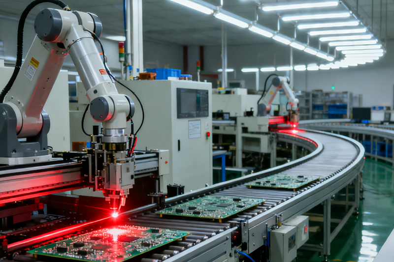
Over the years, we have continuously invested in advanced equipment, process optimization, and engineering expertise to support complex, high-reliability applications.

Today, we serve global clients in telecommunications, industrial control, automotive electronics, and IoT, providing end-to-end PCB solutions with consistent quality and fast turnaround.

0+

Years Experience

0+

Projects Delivered

0+

Global Clients

PCB Manufacturing
ISO 9001 Certified

Our Core Values

The foundation of our engineering excellence and global trust

Innovation

Continuous Innovation

We invest in advanced PCB technologies including HDI, high-frequency materials, and automated manufacturing to stay ahead of industry evolution.

Quality

Uncompromised Quality

From material selection to final inspection, every PCB is manufactured under strict quality control standards to ensure reliability and consistency.

Collaboration

Client-Centric Collaboration

We work closely with engineers and procurement teams to deliver tailored PCB solutions that meet exact project requirements.

Excellence

Engineering Excellence

Our team is committed to precision, performance, and continuous improvement across design, fabrication, and assembly processes.

contact US

Our Engineering Team

Experienced professionals driving precision PCB solutions worldwide

Michael Chen

Michael Chen

Chief Technology Officer

15+ years in PCB design & high-speed signal integrity

Expert in HDI, RF PCB, and complex multilayer stackup design. Leading innovation and engineering excellence.

Sarah Johnson

Sarah Johnson

Head of Manufacturing

Specialist in PCB fabrication & process control

Oversees production quality, yield optimization, and ensures strict compliance with global manufacturing standards.

David Rodriguez

David Rodriguez

Lead PCB Designer

Expert in RF & high-speed PCB layout

Focused on signal integrity, impedance control, and high-frequency PCB optimization for advanced applications.

Our Journey

Key milestones shaping our global PCB expertise

2011

Company Founded

Started as a PCB design studio serving local engineering teams.

2012

Manufacturing Expansion

Added PCB fabrication to deliver full-service solutions.

2015

ISO 9001 Certified

Achieved international quality management certification.

2018

Advanced HDI Technology

Introduced high-density interconnect PCB capabilities.

2021

Global Expansion

Serving clients across North America, Europe, and Asia.

2023

5G & IoT Focus

Specialized PCB solutions for high-frequency applications.

Get a Quote

By The Numbers

Trusted by global clients with proven engineering results

0+

Years of Experience

Deep industry expertise

0+

Projects Delivered

Across multiple industries

0+

Global Clients

Worldwide partnerships

0%

Client Satisfaction

Long-term cooperation rate

Ready to Start Your Next PCB Project?

Work with an experienced PCB manufacturer trusted by global clients. From prototype to mass production, we deliver precision, quality, and fast turnaround.

  • ✔ 15+ Years PCB Experience
  • ✔ ISO 9001 Certified Manufacturing
  • ✔ Fast Response Within 12 Hours

Quick Inquiry

Or chat with us instantly:

💬 WhatsApp Us
WhatsApp