Our PCB Product Portfolio
Explore our comprehensive range of PCB technologies and solutions


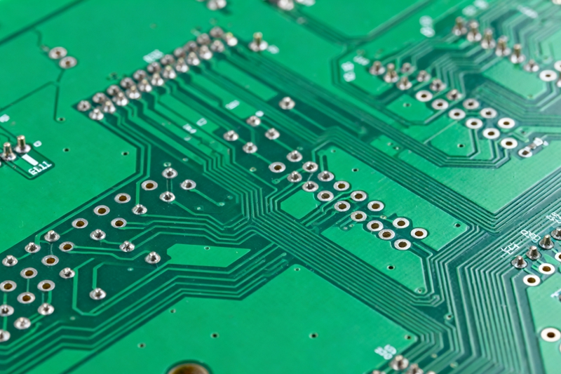
From prototype to mass production — high-reliability PCB manufacturing with fast turnaround and competitive pricing
Explore our comprehensive range of PCB technologies and solutions
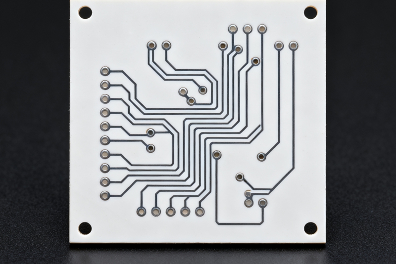
Advanced PCB fabrication capabilities with precise engineering control
Precision-driven workflow ensuring consistent quality at every stage
DFM analysis, stackup planning, impedance simulation
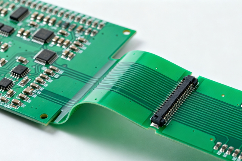
FR4, Rogers, metal core selection based on application
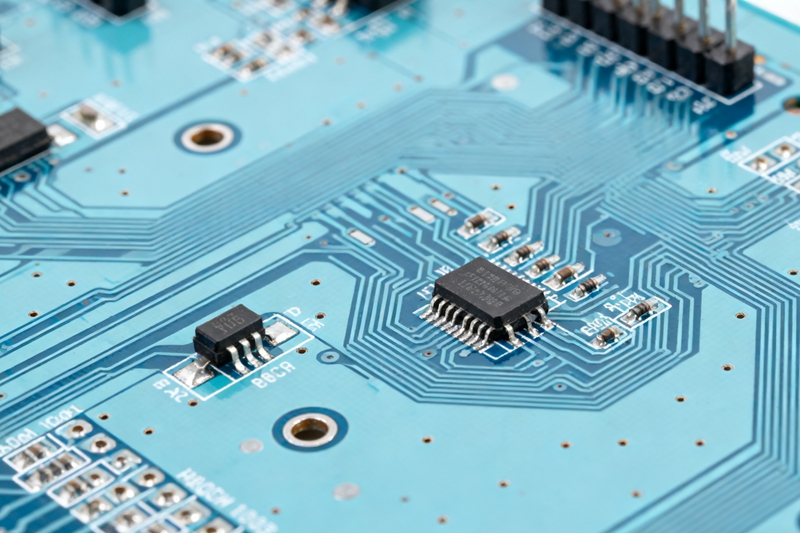
Drilling, plating, etching with high precision equipment
AOI, flying probe test, impedance validation
Secure packaging and global logistics support
Certified processes and advanced inspection systems ensure reliable PCB performance
 ISO 9001
 RoHS Compliant
 IPC Class II/III
 UL Certified
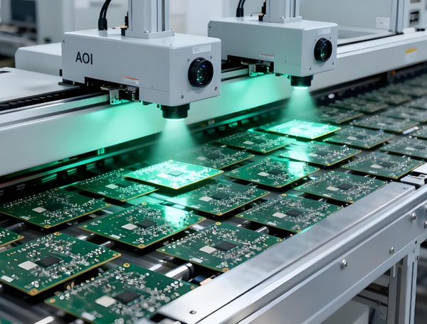
Automated optical inspection for soldering and trace defects
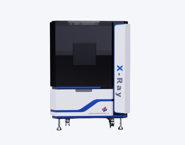
Detect hidden solder joints and BGA integrity
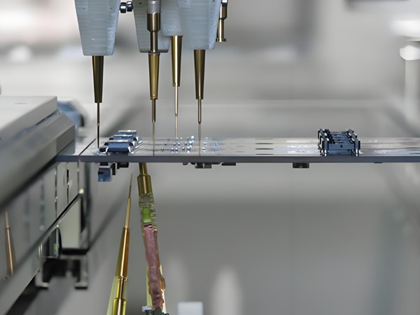
100% electrical testing without fixtures
Our PCB manufacturing meets strict quality standards for automotive, industrial, medical, and communication industries worldwide.
Everything you need to know about our PCB manufacturing services
Standard lead time is 3–7 working days for prototypes and 7–15 days for mass production depending on board complexity.
We support Gerber (RS-274X), ODB++, IPC-2581, and complete PCB design packages.
No strict MOQ. We support both low-volume prototyping and high-volume production.
Yes, we provide impedance control within ±5% and support high-frequency materials such as Rogers and PTFE.
Yes, we offer one-stop PCBA services including SMT, THT, sourcing, and full functional testing.
Fast quotation, expert engineering support, and reliable PCB manufacturing — all in one place.