Multilayer PCB Design Guide: Stackup, Routing, and Manufacturing Considerations
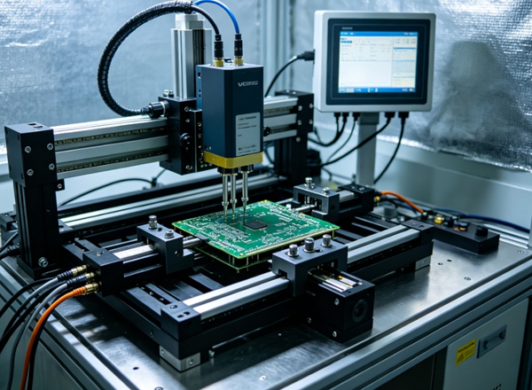
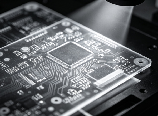
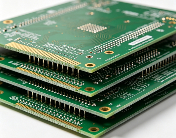
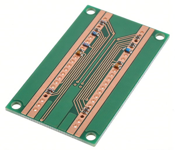
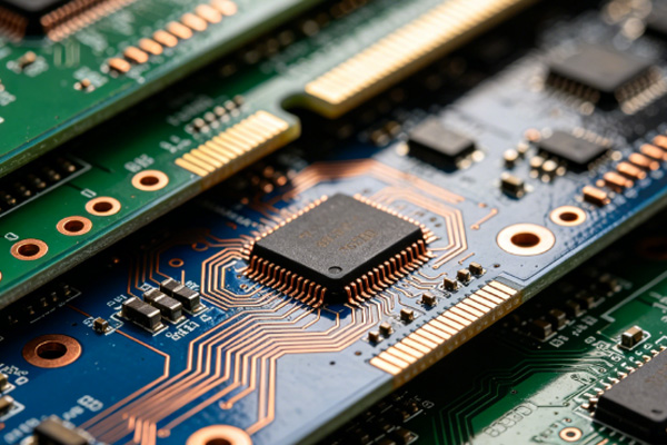
Multilayer PCBs are widely used in modern electronics to support high-density routing, controlled impedance, and stable power distribution. This article explains multilayer PCB stackups, design considerations, and how layer count…