Vias are easy to ignore when routing.
They’re just vertical connections—until they start breaking your signal.
At low speeds, vias behave almost ideally.
At high speeds, they introduce:
- impedance discontinuities
- reflections
- additional insertion loss
Most of the trouble comes from something called a via stub.
What Is a PCB Via?
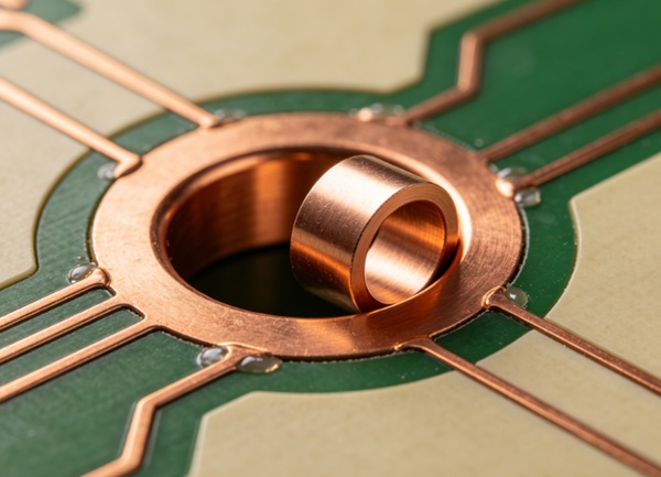
A via is a plated hole that connects different layers of a PCB.
Common types:
- through-hole via (top to bottom)
- blind via (outer to inner layer)
- buried via (inner layers only)
Electrically, a via is not just a connection—it behaves like a small transmission structure.
What Is a Via Stub?
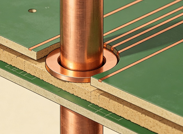
A via stub is the unused portion of a via that extends beyond the signal layer.
Example:
- signal goes from Layer 1 → Layer 3
- via continues down to Layer 8
- the unused section (Layer 3 → 8) is the stub
This stub acts like a resonant structure.
Why Via Stubs Are a Problem
At high frequency, the stub behaves like an open-ended transmission line.
This creates:
- reflections
- resonance at certain frequencies
- signal distortion
In measurements, this often shows up as:
- dips in insertion loss
- unexpected impedance changes
Related concept: PCB Insertion Loss Explained (Dielectric Loss vs Conductor Loss)
When Do Via Stubs Matter?
Not every design needs to worry about them.
They become important when:
- data rates are high (multi-Gbps)
- signal edges are very fast
- layer count is large (longer vias)
In lower-speed designs, the effect is usually negligible.
Backdrilling (How It Fixes the Problem)
Backdrilling removes the unused portion of the via.
Process:
- drill the via normally
- then drill from the opposite side to remove the stub
Result:
- shorter effective via
- reduced reflection
- improved signal integrity
Backdrill vs No Backdrill
| Aspect | Without Backdrill | With Backdrill |
|---|---|---|
| via stub | present | removed |
| reflections | higher | lower |
| insertion loss | higher | lower |
| cost | lower | higher |
Backdrilling adds cost—but often solves real SI problems.
Other Ways to Reduce Via Impact
Backdrilling is not the only option.
1. Use Blind/Buried Vias
These avoid long stubs entirely.
- better signal performance
- higher manufacturing cost
2. Minimize Layer Transitions
Each via adds discontinuity.
Fewer transitions → better signal quality.
3. Optimize Anti-Pad Size
The clearance around the via (anti-pad) affects impedance.
- too small → higher capacitance
- too large → impedance mismatch
4. Use Via-in-Pad (When Needed)
Common in high-density designs.
- short signal path
- reduced inductance
But requires proper filling and plating.
Via Design and Impedance
A via is not impedance-neutral.
It introduces:
- capacitance (to planes)
- inductance (through barrel)
This creates an impedance discontinuity.
In high-speed designs, vias are often modeled and tuned just like traces.
Stackup interaction: FR4 PCB Stackup Design Guide
Via and Return Path
Return current must follow the signal through the via transition.
If there is no nearby reference via:
- return path is broken
- loop area increases
- noise increases
Solution:
- place ground vias near signal vias
More details: PCB Return Path and Ground Plane in High-Speed Design
How to Design Vias for High-Speed PCBs
This is where most improvements happen.
- 1. Keep Vias Short
Shorter vias → less inductance → less reflection
- 2. Avoid Unused Stub Length
Use:
. backdrilling
. blind/buried vias - 3. Place Ground Vias Nearby
Maintain a continuous return path.
- 4. Control Via Geometry
Parameters that matter:
. drill size
. pad size
. anti-pad size - 5. Simulate Critical Vias
For high-speed channels:
. include vias in simulation
. don’t assume they are negligible
Practical Design Notes
From real designs:
- via stubs often show up as unexplained loss spikes
- backdrilling is common in high-speed backplanes
- ignoring return path vias causes EMI issues
- via design matters more as data rate increases
Conclusion
In high-speed PCB design, vias are no longer “just connections.”
They introduce impedance discontinuities and can significantly affect signal integrity. Via stubs, in particular, can cause reflections and resonance issues at high frequencies.
Careful via design—including backdrilling, geometry control, and proper return path planning—is essential for reliable high-speed performance.
FAQ
A: It is the unused portion of a via that extends beyond the signal layer.
A: They act as resonant structures and cause signal reflections.
A: A process that removes the unused part of a via to improve signal integrity.
A: No. It is mainly used in high-speed designs where via stubs affect performance.
A: They introduce capacitance and inductance, creating impedance discontinuities.