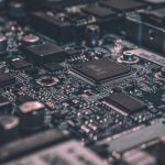
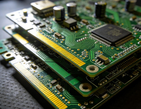
In the realm of high-speed electronics, the PCB substrate is no longer a passive carrier—it is a sophisticated dielectric component. At frequencies above 5GHz, standard FR-4 begins to act like a “signal sponge,” absorbing energy and distorting wave-fronts.
To build a reliable High Frequency PCB, engineers must balance thermal stability, manufacturing yield, and electromagnetic physics. Here is how Hansphere approaches material-first design.
1. Material Selection: Matching the Laminate to the Application
Not every high-speed project requires $50/lb material. The key is matching the Dissipation Factor (Df) to your signal’s Nyquist frequency.
The Material Hierarchy:
- Standard Loss (FR-4): Best for control boards and low-speed digital.
- Mid-Loss (e.g., Isola FR408HR): The “sweet spot” for PCIe Gen3/4 and 10G Ethernet.
- Low Loss (e.g., Panasonic Megtron 6): Mandatory for 25Gbps+ SerDes, AI accelerators, and high-end servers.
- Ultra-Low Loss / RF (e.g., Rogers 4350B/4003C): Essential for 5G mmWave and High Frequency PCB RF front-ends where $Dk$ stability over temperature is critical.
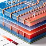
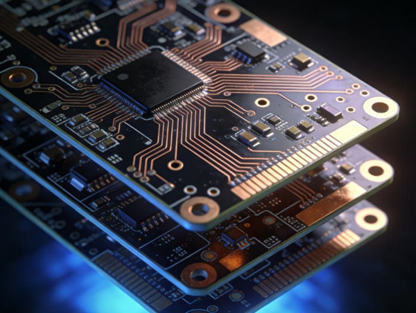
2. Strategic Stackup Engineering
A well-engineered stackup is the first line of defense against EMI. It dictates the characteristic impedance and the return path of every high-speed net.
The “Symmetry & Coupling” Framework:
- Symmetry: The stackup must be physically symmetrical around the core to prevent “warpage” during PCB Assembly.
- Tight Dielectric Coupling: Keep the distance between the signal layer and its reference ground plane as thin as possible (typically 3-5 mils). This confines the electromagnetic field and reduces crosstalk.
- Ground Plane Continuity: High-speed signals should never transition across a split in the reference plane.
5 Steps to Finalize a High-Speed Stackup
Target: Hardware Architects & SI Engineers
Focus: Balancing Performance and Fabricatability
- Step 1: Define Your Impedance Targets
Identify your critical nets (e.g., 90Ω USB, 100Ω PCIe, 50Ω Single-ended). Use an electromagnetic field solver to determine the required trace widths for your chosen material.
- Step 2: Select the Core and Prepreg
Choose materials with consistent Dk (Dielectric Constant). For HDI-PCB, ensure the prepreg is compatible with laser drilling.
- Step 3: Map the Signal-Return Path
For every signal layer, there must be an adjacent ground plane. In 2026, “Ground-Signal-Signal-Ground” configurations are common, but they require careful “Orthogonal Routing” between the two signal layers to prevent broadside coupling.
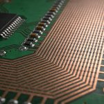
- Step 4: Verify Copper Foil Profile
At high frequencies, the “Skin Effect” pushes current to the surface of the copper. Rough copper creates more resistance and loss. Specify Very Low Profile (VLP) or Hyper-Very Low Profile (HVLP) copper for signals above 10Gbps.
- Step 5: Consult with Hansphere DFM
Before freezing the design, send your stackup to our engineers. We verify that the materials are in stock and that the resin content is sufficient to fill the copper voids during PCB Manufacturing.
3. Advanced Considerations: Thermal and Hybrid Stackups
- Thermal Management: High-speed chips run hot. Consider using Thermal Vias or even a Ceramic PCB base if your application involves high-power RF amplifiers.
- Hybrid Stackups: To save costs, you can use high-speed materials (like Rogers) only on the top layers where the RF signals live, while using standard FR-4 for the internal low-speed layers.
FAQ – High-Speed PCB Stackup and Materials
A: At high speeds, the signal can “see” the gaps in the fiberglass weave, causing skew. Use “Spread Glass” (like 1067 or 1078 weave) or route your traces at a slight angle (zigzag) to average out the $Dk$ variations.
A: FR-4 can support many high-speed designs, but higher data rates may require low-loss laminates.
A: Dk determines the signal velocity. A lower Dk means signals travel faster and traces can be wider for the same impedance, which reduces skin-effect losses.
A: Yes. For every Rigid PCB or high-speed board, we provide a full TDR test report and a certificate of compliance for your stackup specifications.
Conclusion
Stackup and material selection are the “Invisible Engineering” that makes high-speed digital possible. By choosing the right resin system, copper profile, and layer sequence, you create a stable environment where signals can thrive without interference.
Need a Precision Stackup? Don’t guess your impedance. Hansphere’s Engineering Team specializes in complex, high-layer count stackups with exotic materials. Contact us for a Stackup Review today.