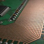
One of the most common misunderstandings in PCB design is thinking that current flows “from point A to point B” along the trace—and that’s it.
That’s only half the story.
Every signal has a return path, and at high speed, that return path is just as important as the signal trace itself.
If the return path is poorly defined, you’ll see:
- impedance issues
- EMI problems
- unexpected noise
- signal integrity degradation
This is why ground planes matter more in high-speed design than in low-speed circuits.

What Is a Return Path?
A return path is the path that current takes to complete the circuit back to the source.
At low frequency:
- current tends to follow the path of least resistance
At high frequency:
- current follows the path of least impedance
- which usually means closest to the signal trace
In practice, this means return current flows directly under the trace—on the nearest reference plane.
Why Ground Planes Matter
A solid ground plane provides a clean, low-impedance return path.
This has several effects:
- stabilizes impedance
- reduces loop area
- lowers EMI radiation
- improves signal integrity
Without a continuous reference plane, the return current has to “find another way,” which usually means larger loops and more noise.
What Happens When the Return Path Is Broken
This is where problems start.
If a signal crosses:
- a split plane
- a gap in ground
- a via transition without proper stitching
the return current is forced to detour.
That detour creates:
- larger current loops
- increased EMI
- impedance discontinuities
In real boards, this shows up as:
- failing EMI tests
- unstable high-speed signals
- unexpected ringing
Return Path and Loop Area
The loop formed by:
- signal trace
- return path
is critical.
Larger loop area → stronger radiation → more EMI
Keeping the return path directly under the signal minimizes loop area and reduces emissions.
Relationship to Impedance Control
Controlled impedance depends on the interaction between:
- the signal trace
- the reference plane
If the return path is disrupted:
- impedance is no longer stable
- reflections can occur
This ties directly into stackup design.
See FR4 PCB Stackup Design Guide.
Return Path and Signal Integrity
Many high-speed problems trace back to poor return paths:
- jitter
- crosstalk
- waveform distortion
Even if trace routing looks correct, ignoring the return path can break the design.
For loss-related effects, see PCB Insertion Loss Explained (Dielectric Loss vs Conductor Loss).
How to Design a Proper Return Path
This is where most practical improvements happen.
- 1. Always Route Over a Continuous Reference Plane
Signal traces should always have a solid ground (or power) plane directly beneath them.
Avoid routing over:
plane splits
voids
cutouts - 2. Keep Signal and Return Path Close
The closer the signal is to its reference plane:
the tighter the coupling
the smaller the loop area
the better the signal integrity - 3. Use Ground Planes Instead of Ground Traces
A wide copper plane provides a much lower impedance path than a thin trace.
For high-speed designs:
planes are preferred
traces are not sufficient - 4. Add Stitching Vias When Changing Layers
When a signal transitions between layers:
the return path must also transition
Use ground vias near signal vias to maintain a continuous return path. - 5. Avoid Splitting Ground Planes
Split planes force return currents to detour, increasing loop area and noise.
If splits are unavoidable:
provide bridging capacitors
or redesign the routing
Return Path in Differential Pairs
Differential signals behave slightly differently.
Most of the return current flows:
- between the two traces
But the reference plane still matters for:
- impedance stability
- EMI control
So even for differential pairs, a solid reference plane is still required.
Interaction with High-Frequency Effects
Return path behavior is tightly linked with:
- skin effect → current crowding
- insertion loss → signal attenuation
- dielectric properties → impedance stability
Related topics:
Practical Design Notes
A few things that come up often in real layouts:
- routing across plane splits is a common source of EMI failure
- missing stitching vias can break return paths silently
- power planes can act as return paths—but only if properly decoupled
- “it works at low speed” does not mean it works at high speed
Conclusion
In high-speed PCB design, signals do not exist without return paths.
A well-designed ground plane provides a stable, low-impedance path that supports signal integrity and reduces EMI. Poor return path design, on the other hand, can introduce noise, reflections, and unpredictable behavior.
Understanding how return current flows is one of the most important steps toward reliable high-speed PCB design.
FAQ
A: It is the path current takes to return to the source, completing the electrical loop.
A: Because it directly affects impedance, EMI, and signal integrity.
A: Not always, but in most PCB designs, the return path flows through the nearest reference plane.
A: It can cause EMI issues, impedance discontinuities, and signal degradation.
A: Yes. Even though current flows between the pair, a reference plane is still needed for stable performance.