If high-speed design starts anywhere, it starts with the stackup.
Not routing. Not placement.
Stackup.
Once the layer structure is fixed, most of your electrical behavior is already constrained:
- impedance
- return path
- crosstalk
- loss
Trying to “fix” these later in layout is usually painful.
What Stackup Really Controls
A PCB stackup defines:
- where signals are routed
- where reference planes are placed
- how fields are contained
In practice, it determines:
- impedance stability
- EMI performance
- routing flexibility
If the stackup is weak, everything downstream becomes harder.
Basics: FR4 PCB Stackup Design Guide
Typical 6-Layer Stackup
A common 6-layer structure:
L1  Signal
L2  Ground
L3  Signal
L4  Signal / Power
L5  Ground
L6  Signal
Where it works
- moderate-speed designs
- cost-sensitive products
- limited routing density
Limitations
- fewer reference planes
- more signal layers competing for routing
- harder to isolate noisy signals
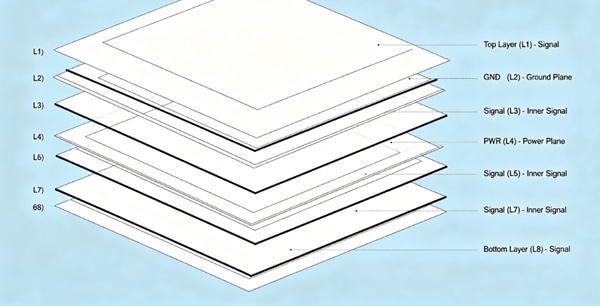
Typical 8-Layer Stackup
A common 8-layer structure:
L1  Signal
L2  Ground
L3  Signal
L4  Power
L5  Ground
L6  Signal
L7  Ground
L8  Signal
Advantages
- better signal/plane pairing
- improved return path control
- reduced crosstalk
Practical impact
Most high-speed designs start to feel “comfortable” at 8 layers.
Typical 10-Layer Stackup
A common 10-layer structure:
L1  Signal
L2  Ground
L3  Signal
L4  Ground
L5  Signal
L6  Signal
L7  Ground
L8  Signal
L9  Ground
L10 Signal
Advantages
- excellent signal isolation
- more routing channels
- strong EMI performance
Trade-offs
- higher cost
- more complex fabrication
6 vs 8 vs 10 Layers (Quick Comparison)
| Feature | 6-Layer | 8-Layer | 10-Layer |
|---|---|---|---|
| impedance control | basic | stable | very stable |
| crosstalk control | limited | good | excellent |
| routing density | moderate | high | very high |
| EMI performance | moderate | good | strong |
| cost | lower | medium | higher |
How Layer Count Affects Signal Integrity
1. Return Path Quality
More planes → better return paths
See: PCB Return Path and Ground Plane in High-Speed Design
2. Crosstalk
More spacing + better shielding → less coupling
See: PCB Crosstalk Explained (Near-End vs Far-End Crosstalk)
3. Impedance Stability
More controlled dielectric spacing → more consistent impedance
See: Controlled Impedance PCB Design: How to Achieve 50Ω and 100Ω
4. Insertion Loss
Indirect effect:
- better routing → shorter paths
- cleaner structure → fewer discontinuities
See: PCB Insertion Loss Explained (Dielectric Loss vs Conductor Loss)
How to Choose Between 6, 8, and 10 Layers
This is usually not just a technical decision—it’s a trade-off.
- 1. Look at Signal Speed First
low–mid speed → 6 layers may work
high-speed / multi-Gbps → 8 or more - 2. Evaluate Routing Density
If routing is congested:
adding layers is often easier than forcing layout - 3. Check Power Distribution Needs
More planes → better power integrity
- 4. Consider EMI Requirements
Stricter EMI → more layers + better shielding
- 5. Balance Cost vs Risk
Fewer layers save cost—but increase design risk.
More layers increase cost—but simplify SI/EMI control.
How to Build a Good High-Speed Stackup
This is where designs succeed.
1. Pair Signal Layers with Planes
Every signal layer should have a nearby reference plane.
2. Use Symmetrical Structures
Balanced stackups reduce warping and improve manufacturability.
3. Keep Dielectric Thickness Consistent
Helps maintain stable impedance.
4. Separate High-Speed and Noisy Signals
Use different layers or shielding planes.
5. Plan Via Transitions Early
Layer changes introduce discontinuities.
Details: PCB Via Design in High-Speed Circuits
Microstrip vs Stripline in Stackup
- outer layers → microstrip
- inner layers → stripline
Stripline advantages:
- less EMI
- better shielding
- more stable impedance
High-speed signals are often routed on inner layers for this reason.
Practical Design Notes
What usually happens in real projects:
- 6-layer designs often become 8-layer after SI review
- 8-layer is the “sweet spot” for many products
- 10-layer is common for high-density or high-speed systems
- stackup decisions made early save redesign time later
Conclusion
Stackup design defines the electrical behavior of a high-speed PCB.
While 6-layer boards can work for simpler designs, 8-layer and 10-layer structures provide better control over impedance, return paths, and crosstalk.
Choosing the right layer count is a balance between performance, routing complexity, and cost—but getting the stackup right early makes everything else easier.
FAQ
A: It can be, but it becomes harder to control impedance and crosstalk compared to 8-layer designs.
A: It provides a good balance between performance, routing flexibility, and cost.
A: For high-speed, high-density, or EMI-sensitive designs.
A: Not always, but more layers usually make it easier to control signal integrity.
A: Yes. Stackup should be defined before layout begins.