Once signals start switching fast enough, they don’t stay isolated.
Put two traces close together, and energy from one line will couple into the other. That’s crosstalk.
At low speeds, it’s usually negligible.
At high speeds, it shows up as:
- noise on quiet lines
- timing issues
- eye diagram closure
If you’ve already looked at return paths and impedance, crosstalk is the next piece of the puzzle.

What Is Crosstalk?
Crosstalk is unwanted coupling between adjacent signal traces.
It happens because of:
- electric field coupling (capacitive)
- magnetic field coupling (inductive)
The closer and longer two traces run together, the stronger the coupling.
Near-End vs Far-End Crosstalk
Crosstalk is usually divided into two types.
Near-End Crosstalk (NEXT)
Measured at the same end as the signal source.
- appears immediately
- usually stronger
- common in parallel routing
Far-End Crosstalk (FEXT)
Measured at the far end of the victim trace.
- depends on signal propagation
- affected by trace length and timing
- can partially cancel out depending on geometry
Quick Comparison
| Type | Where Measured | Behavior | Typical Impact |
|---|---|---|---|
| NEXT | near source | immediate | stronger noise |
| FEXT | far end | delayed | depends on length |
In most digital systems, NEXT is the primary concern.
What Causes Crosstalk in PCBs
In real layouts, a few factors dominate:
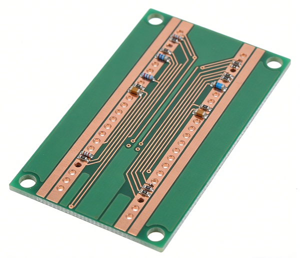
1. Trace Spacing
Closer traces → stronger coupling
This is usually the biggest factor.
2. Parallel Routing Length
The longer two traces run side by side, the more energy couples.
Short parallel sections are usually fine. Long ones are not.
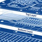
3. Stackup and Reference Planes
Poor return paths increase field spreading, which increases coupling.
A solid reference plane helps confine fields and reduce crosstalk.
More on this: PCB Return Path and Ground Plane in High-Speed Design
4. Signal Rise Time
Faster edges → higher frequency content → more coupling
Even if your clock frequency is moderate, fast edges can still create problems.
How Crosstalk Relates to Impedance and Return Path
Crosstalk is not an isolated issue.
It’s closely tied to:
- impedance control
- return path integrity
- dielectric properties
For example:
- poor return path → wider field distribution → more coupling
- unstable impedance → reflections → additional noise
Related reading:
- FR4 Dielectric Constant (Er) vs Frequency Explained
- PCB Insertion Loss Explained (Dielectric Loss vs Conductor Loss)
How to Reduce Crosstalk in PCB Design
This is mostly layout discipline.
- 1. Increase Trace Spacing
The simplest rule:
spacing ≥ 3× trace width (3W rule)
More spacing = less coupling. - 2. Reduce Parallel Routing Length
Avoid running high-speed signals side by side for long distances.
If they must cross:
cross at 90° when possible - 3. Use Solid Reference Planes
A continuous ground plane keeps fields contained and reduces coupling.
Details: FR4 PCB Stackup Design Guide - 4. Route Critical Signals on Inner Layers
Stripline structures (between planes) radiate less than surface traces.
This reduces both EMI and crosstalk. - 5. Use Ground Guard Traces (When Necessary)
Ground traces between signals can help, but only if:
.properly stitched with vias
.connected to a solid reference plane
Otherwise, they can make things worse. - 6. Control Edge Rates
If possible, avoid unnecessarily fast rise times.
Slower edges → less high-frequency content → less coupling.
Crosstalk in Differential Pairs
Differential pairs behave differently:
- signals are tightly coupled to each other
- external coupling is reduced
But:
- poor spacing between pairs still causes interference
- imbalance can convert noise into common-mode signals
So spacing rules still apply between pairs.
Practical Design Notes
Things that show up often in real boards:
- spacing fixes more problems than people expect
- long parallel routing is usually the root cause
- moving one trace to another layer can solve the issue
- crosstalk often appears only after increasing data rate
Conclusion
Crosstalk is a natural result of electromagnetic coupling between traces.
In high-speed PCB design, it becomes a practical issue that affects signal integrity and system reliability. Managing spacing, routing, and stackup design is the most effective way to control it.
Like most SI problems, it’s easier to prevent than to fix later.
FAQ
A: It is unwanted signal coupling between adjacent traces.
A: NEXT appears at the source end, while FEXT appears at the far end of the victim trace.
A: Increase spacing, reduce parallel routing, and use solid reference planes.
A: Not at low speeds, but it becomes significant in high-speed designs.
A: No, but they are more resistant compared to single-ended signals.