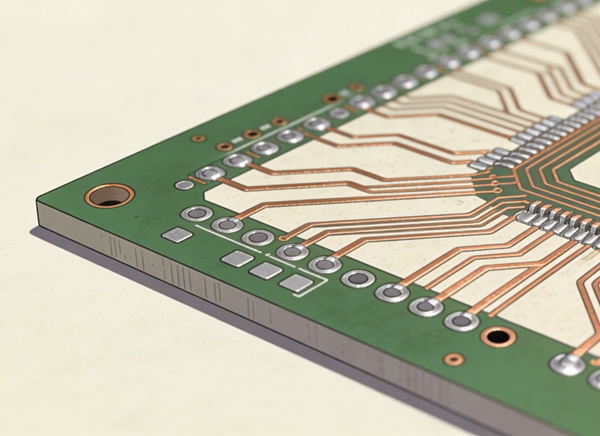
In modern electronics, a PCB stackup is much more than a sandwich of copper and fiberglass. It is a complex network of transmission lines where the spacing between layers dictates the impedance, and the sequence of layers determines the board’s susceptibility to noise.
At Hansphere, we’ve found that 80% of EMI issues can be traced back to poor layer planning. Here is how to architect a Rigid PCB that is both electrically quiet and mechanically robust.
1. The Fundamental Principles of Stackup Design
To ensure signal integrity, every high-speed layer must be adjacent to a solid reference plane (Ground or Power). This creates a “Return Path” for the current, minimizing the loop area.
The Rules of Professional Planning:
- Symmetry is Key: The stackup must be mirrored around the center core. If you use a 5-mil dielectric between layers 1-2, you must use a 5-mil dielectric between the last two layers. Failure to do so leads to “Potato Chipping” (warping) during PCB Assembly.
- Tight Coupling: The distance between a signal layer and its return plane should be as small as possible (ideally ≤ 5 mils) to confine the electromagnetic fields.
- Plane Pairing: Power and Ground planes should be placed as close together as possible to create “Interplane Capacitance,” which helps filter high-frequency power noise.
2. Standard Stackup Templates
The 4-Layer Classic (Signal-Ground-Power-Signal)
This is the most common entry-level multi-layer board. By keeping the internal layers as planes, you provide excellent shielding for the signal traces on the outer layers.
The 6-Layer Performance (Signal-Ground-Signal-Signal-Power-Ground)
A 6-layer board allows for two dedicated internal signal layers.
- Expert Tip: To avoid crosstalk between the internal signal layers (Layers 3 and 4), route them orthogonally (one horizontally, one vertically).
High-Layer Count (8+ Layers)
For High-Speed PCB Design, 8 or more layers are often required to provide enough ground isolation between sensitive analog and noisy digital sections.
5 Steps to Finalizing a Production-Ready Stackup
Target: System Designers & Layout Engineers
Focus: Balancing Electrical Performance with Fabrication Costs
- Step 1: Determine Total Signal Count
Count your high-speed nets, power rails, and control signals. This dictates the minimum number of layers required to avoid a “routing bottleneck.”
- Step 2: Select the Core and Prepreg Materials
Not all FR-4 is the same. For high-reliability rigid boards, specify High-Tg (Glass Transition Temperature) materials to ensure the vias don’t crack during lead-free soldering.
Related: See our Material Selection Guide for more. - Step 3: Define Impedance Requirements
Use a field solver (like Polar SI8000) to calculate the trace widths needed for 50Ω or 100Ω nets based on the dielectric thickness. Hansphere provides a free Stackup Calculation Service for all PCB Manufacturing orders.
- Step 4: Verify Thru-Hole Aspect Ratio
Ensure the board thickness divided by the smallest drill size is ≤ 10:1. For example, a 1.6mm board should have drills no smaller than 0.16mm to ensure reliable plating. If you need smaller, consider HDI-PCB technology.
- Step 5: Final DFM Check
Check for “Copper Balance.” Ensure that the copper density is roughly even across each layer to prevent uneven etching and mechanical stress.
3. Advanced Features for Rigid Boards
- Edge Plating: Plating the edges of the board to create an EMI “Faraday Cage.”
- Embedded Capacitance: Using ultra-thin dielectrics between power/ground planes to boost PDN performance.
- Mixed Construction: Combining standard FR-4 with high-frequency materials like Rogers for High Frequency PCBs.
Frequently Asked Questions (FAQ)
A: Odd-layer counts are inherently asymmetrical. This causes the board to warp severely during the thermal cycles of PCB Assembly. It also increases manufacturing costs because the process is non-standard.
A: Core is a cured piece of FR-4 with copper on both sides. Prepreg is “pre-impregnated” bonding material that is uncured and acts as the “glue” that holds the layers together during lamination.
A: Yes. Often, a design can be condensed from 8 layers to 6 layers by using finer traces or smarter plane placement. Our About Us page highlights our precision LDI equipment that allows for these tighter tolerances.
Conclusion
Stackup planning is the foundation of high-performance hardware. A well-thought-out layer plan reduces noise, improves power delivery, and ensures your board can be manufactured with high yield.
Ready to Build Your Multi-Layer Board? Hansphere specializes in high-layer count Rigid PCBs with complex impedance requirements. Request a Custom Stackup Review today and get your design started on the right path.