ISO 9001 Certified · Shenzhen, China

High-complexity PCBs,
engineered for reliability.

From 48-hour HDI prototypes to full turnkey production — DFM on every order, IPC Class 2/3 default, DDP to 40+ countries.

48h Express 30-Layer Capability DDP · 40+ Countries
Get a Quote in 8 Hours No commitment  ·  DFM included  ·  NDA available
0+
Years Experience
0+
Projects Delivered
0%
On-Time Delivery
0%
First-Pass Yield
What We Do

One-Stop PCB Solutions

From design to mass production, we support your entire product lifecycle

PCB Design Services

Professional PCB layout services for complex electronics. Our senior engineers deliver high-speed, RF and mixed-signal designs with full signal integrity analysis and DFM-ready output.

  • High-speed & RF design
  • HDI & multilayer layout
  • Signal integrity analysis
  • Impedance control & DFM review
Get Design Quote

PCB Manufacturing

Precision PCB fabrication in our ISO 9001 certified facility. From prototypes to high-volume production, we deliver consistent quality across 2–32 layer boards in a variety of advanced materials.

  • HDI / High Frequency PCB
  • Rogers / FR4 / Ceramic materials
  • 2–32 layer stackup capability
  • 48h prototype available
Start Manufacturing

PCB Assembly

Complete SMT and THT assembly services with AOI, X-ray inspection, and functional testing. From small prototypes to large production runs, all assemblies meet IPC Class II/III standards.

  • SMT & THT assembly
  • AOI / X-ray inspection
  • BGA rework & functional testing
  • IPC Class II / III workmanship
Request Assembly

Turnkey PCBA

Complete end-to-end PCB solutions from design and component sourcing through final assembly and delivery. We manage everything so you can focus on your product, not your supply chain.

  • Global component sourcing
  • Full assembly & testing
  • Box-build & integration
  • One-stop quality assurance
Learn About Turnkey
Why HanSphere

Engineering Excellence
You Can Trust

We combine deep technical expertise with end-to-end capability, rigorous quality, and fast execution — so your next PCB project moves from concept to volume without friction.

Get Instant Quote

Technical Expertise

Senior engineers with deep experience in HDI, high-speed, RF, and mixed-signal PCB design across demanding industries.

Full-Range Capability

From 2-layer boards to 32-layer HDI, flexible, rigid-flex, and ceramic PCBs — all manufactured under one roof for full accountability.

Quality Assurance

ISO 9001 certified processes with AOI, X-ray, and flying-probe testing for every order. IPC Class II/III workmanship as standard.

Rapid Turnaround

48-hour prototypes and streamlined production workflows — we accelerate your time-to-market without compromising on quality.

Our People

Professional PCB Engineering Team

Experienced engineers delivering reliable and high-performance PCB solutions

15+ Years PCB Expertise

Our engineering team specializes in PCB design, manufacturing, and assembly, covering everything from simple boards to complex HDI and high-speed designs.

  • Altium Designer / Cadence Allegro / Mentor PADS
  • High-speed, RF & mixed-signal design
  • Signal integrity & impedance control
  • DFM / DFA optimization support
Talk to Our Engineers →
Lead PCB Designer
PCB Design

Lead PCB Designer

Signal Integrity Specialist
Manufacturing Engineer
Manufacturing

Manufacturing Engineer

Quality Assurance Lead
Assembly Specialist
Assembly

Assembly Specialist

Technical Support Manager
Why HanSphere

Built for engineers,
trusted by 500+ companies worldwide.

We combine engineering depth, in-house capacity and transparent process to deliver boards you can rely on — from prototype to production.

Get Instant Quote →
100%
DFM coverage

Every board design-reviewed

Stack-up, trace width, impedance and DRC checked before production. Included with every order, no extra charge.

15yr
average seniority

Senior engineering team

Direct access to SI, RF and DFM specialists. Real engineers, not ticket queues — response within 4 working hours.

48h
express prototype

Rush turnaround, global delivery

Standard 5-day lead time. 48h express available. DDP shipping to 40+ countries — one less thing to manage.

IPC 2/3
default build standard

ISO 9001 · IATF 16949

Certified quality system. Every board 100% e-tested, AOI + X-ray inspected before it leaves our facility.

Product Range

Explore Our PCB Types

Diverse PCB solutions engineered for every application

Our Facility

Built for precision
at production scale.

Two plants in Shenzhen, vertically integrated from bare board fabrication to full SMT assembly and functional test — under ISO 9001 certified quality management.

50,000
Total facility floor area across two plants
12 SMT lines
High-speed surface mount lines with AOI
200+ engineers
Production and QA staff on-site
Request a Factory Tour →
50,000 sqm
Factory Floor
200+
Production Staff
ISO 9001
Certified Quality
How It Works

From Gerber to your door —
a process you can count on.

Start Your Project →
01

Inquiry &
DFM Review

Send your Gerber — we return a full DFM report within 8 hours, free of charge.

02

Quote &
NDA

Transparent line-item quote. NDA signed on request — standard practice for all customers.

03

Engineering
Sign-off

Stack-up, controlled impedance, bow & twist — all confirmed before board drops to fab.

04

Fabrication
& Assembly

In-house pressing, plating, SMT, AOI and X-ray — every board 100% electrically tested.

05

DDP Delivery
& Support

Shipped door-to-door worldwide. Engineering support continues after delivery — always.

Industry Solutions

Serving Every Industry

PCB solutions engineered for diverse market applications

Standards & Compliance

Certifications that matter
to your procurement team.

Request Cert Documents →
ISO 9001

ISO 9001 : 2015

Every process documented, audited and traceable — from incoming materials to final test.

UL E-File

UL E-File Listed

Recognised by US and Canadian safety regulators. Required for many consumer and industrial end-products.

RoHS / REACH

RoHS / REACH

EU hazardous substance compliance. Full material declarations available for every board type.

IPC-A-600

IPC-A-600 Class 2/3

Industry-standard acceptability criteria for PCBs. Class 3 available on request for aerospace and medical.

Customer Voice

What engineers say
about working with us.

4.9/5
★★★★★
Based on 340+ verified reviews
Volume Production · 3,000 units
"Consistent first-pass yield above 98% across three production runs. Communication is clear, professional and always in English. Two years in and they're still our go-to PCB partner."
MD
Marc Dubois Production Manager, Systronix GmbH · 🇩🇪 Germany
IPC Class III · Aerospace
"Our avionics boards require IPC Class III compliance and zero-defect tolerance. HanSphere met every specification and delivered ahead of schedule — something very few overseas suppliers can claim."
LA
Lars Andersen Systems Engineer, AeroTech Nordic · 🇸🇪 Sweden
Technical Resources

Engineering Insights

Practical guides and technical deep-dives for hardware engineers

View All Articles →
PCB Power Integrity Design: Decoupling, PDN, and Noise Control PCB Design
April 29, 2026

PCB Power Integrity Design: Decoupling, PDN, and Noise Control

Power integrity (PI) is critical in modern PCB design. Stable power delivery ensures reliable operation of high-speed devices and reduces noise issues. This article explains decoupling strategies, PDN design, and practical techniques to control power noise.

Read More
High-Speed PCB Stackup Design: 6-Layer vs 8-Layer vs 10-Layer
April 27, 2026

High-Speed PCB Stackup Design: 6-Layer vs 8-Layer vs 10-Layer

Stackup design is a critical step in high-speed PCB development. The number of layers directly affects signal integrity, EMI, impedance control, and routing complexity. This article compares 6-layer, 8-layer, and 10-layer stackups and explains how engineers choose the right structure.

Read More
PCB Via Design in High-Speed Circuits: Stub, Backdrilling, and Signal Integrity
April 26, 2026

PCB Via Design in High-Speed Circuits: Stub, Backdrilling, and Signal Integrity

Vias play an important role in multilayer PCB design, but in high-speed circuits they can introduce signal reflections and additional loss. This article explains via stubs, backdrilling, and how engineers design vias to maintain signal integrity.

Read More
FAQ

Frequently Asked Questions

Answers to common questions about our PCB services

What PCB services do you provide? +
We provide one-stop PCB solutions including PCB design, manufacturing, assembly, and testing services for various industries including automotive, medical, aerospace, and consumer electronics.
What is your PCB prototype lead time? +
Our PCB prototype lead time can be as fast as 48 hours depending on complexity and requirements. Standard prototypes are typically delivered within 3–5 business days.
Do you support HDI and high-frequency PCB? +
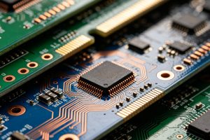
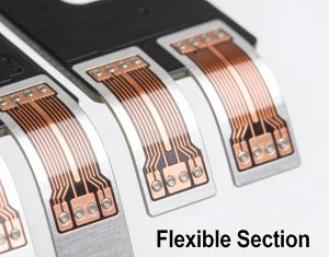
Yes, we specialize in HDI (high-density interconnect), high-frequency, multilayer, and complex PCB solutions. We work with Rogers, PTFE, and other specialty materials for RF and microwave applications.
Can you provide PCB assembly services? +
Yes, we offer full PCB assembly services including SMT, THT, component sourcing, BGA rework, and functional testing. We also provide complete turnkey PCBA solutions.
How do you ensure PCB quality? +
We follow strict quality control processes including automated optical inspection (AOI), X-ray testing, flying probe electrical testing, and compliance with IPC Class II/III standards. Our facility is ISO 9001 certified.
What is your minimum order quantity? +
We accept orders starting from a single prototype board. For mass production, minimum order quantities depend on the PCB type and complexity, but we work flexibly with customers from prototype through high-volume production.
Do you offer DFM review services? +
Yes, Design for Manufacturability (DFM) review is included with every order at no extra charge. Our engineers check your Gerber files and design data to identify potential issues before production begins, preventing costly rework.
Can you handle both prototype and mass production? +
Absolutely. We support the full product lifecycle — from rapid prototyping (48h) to large-scale mass production. Our consistent processes ensure the same quality and specifications are maintained from your first prototype to your millionth unit.
WhatsApp