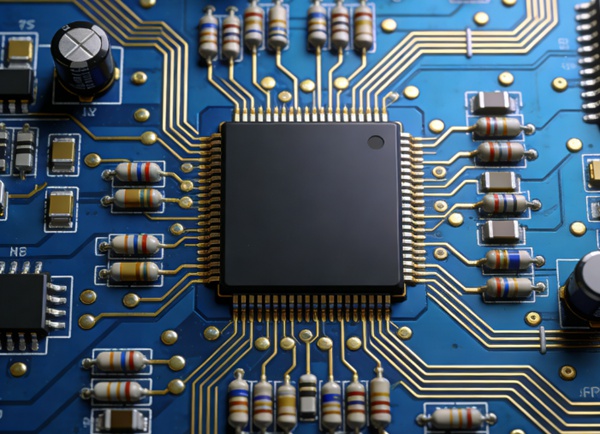
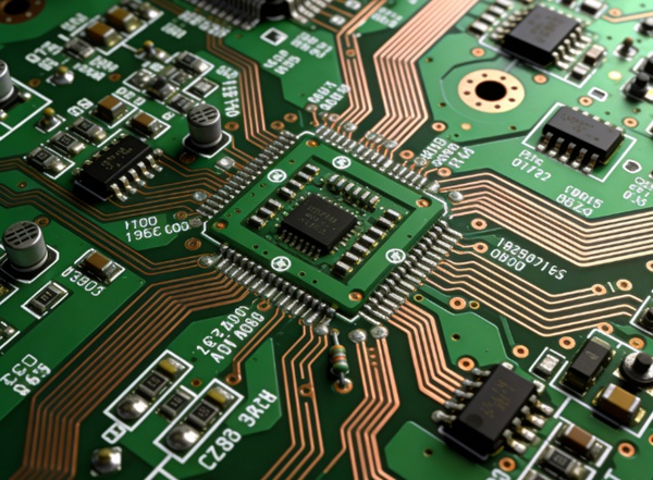
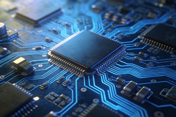
As PCB designs move toward higher speeds, higher densities, and lower voltage margins, signal integrity (SI) and power integrity (PI) have become primary limiting factors in electronic system performance. Traditional simulation-driven workflows remain essential but often require multiple iterations and significant engineering effort.
Machine learning applications in PCB signal integrity and power integrity analysis are increasingly used to complement conventional simulation methods. By learning from historical design data and simulation results, AI-driven approaches help engineers identify risk patterns earlier, reduce iteration cycles, and improve overall design reliability.
🔗 This article is part of the core topic:
AI PCB Design: Practical Applications of Machine Learning in Modern Electronics
Why Signal Integrity and Power Integrity Are Critical in Modern PCB Design
In high-speed PCB design, signal behavior is no longer dominated by simple DC assumptions. Fast edge rates, dense routing, and complex stackups introduce challenges such as:
- Reflections caused by impedance discontinuities
- Crosstalk between closely spaced traces
- Simultaneous switching noise (SSN)
- Power plane resonance and voltage droop
These issues directly impact system reliability in interfaces such as PCIe, DDR memory, high-speed SerDes, and RF-enabled designs.
While traditional SI/PI simulation tools remain the gold standard, they are often applied late in the design process—after layout decisions have already constrained possible solutions.
How Machine Learning Enhances PCB Signal Integrity Analysis
Pattern Recognition in High-Speed Routing
Machine learning models trained on large datasets of routed PCBs and simulation outcomes can identify routing patterns associated with SI failures. Instead of analyzing each net independently, ML-based tools evaluate routing context, including:
- Trace geometry and spacing
- Reference plane continuity
- Via placement and transitions
- Differential pair symmetry
This allows AI systems to flag high-risk signal paths before full-wave simulation is performed.
Predictive SI Risk Assessment
Rather than replacing simulation, machine learning provides early-stage SI risk prediction. For example, AI models can estimate the likelihood of:
- Excessive insertion loss
- Return loss degradation
- Crosstalk-induced jitter
These predictions help engineers prioritize critical nets and focus simulation resources where they are most needed.
🔗 Related layout considerations are discussed in:
How AI Improves PCB Layout and Routing for High-Speed and High-Density Boards
Machine Learning in Power Integrity Analysis
Early Detection of Power Delivery Network Issues
Power integrity problems are often difficult to diagnose late in the design cycle. Machine learning models can analyze PDN topology, decoupling strategies, and stackup parameters to predict:
- Voltage droop under dynamic load
- Resonance frequencies in power planes
- Inefficient decoupling capacitor placement
By identifying risky PDN configurations early, AI-assisted analysis reduces the likelihood of costly redesigns.
Optimizing Decoupling Strategies
Traditional decoupling design relies on experience-based rules and iterative simulation. Machine learning can accelerate this process by recommending capacitor values and placements based on similar, previously validated designs.
This approach improves power distribution efficiency while reducing trial-and-error during PDN optimization.
Limitations and the Need for Validation
Despite its value, machine learning does not eliminate the need for traditional SI/PI simulation or engineering expertise.
Key limitations include:
- Dependence on training data quality
- Reduced accuracy for novel or unconventional designs
- Inability to replace physics-based validation
Machine learning should be used as a decision-support layer, guiding engineers toward better design choices rather than acting as a final authority.
How This Fits into the AI PCB Design Workflow
Machine learning–based SI and PI analysis represents a critical middle layer between layout/routing and final simulation. When combined with AI-assisted placement and routing, it enables a more predictive and efficient PCB design workflow.
🔗 For a broader tool perspective, see:
AI Tools for PCB Design Engineers: Features, Limitations, and Use Cases
🔗 For industry outlook, see:
The Future of AI in PCB Design Automation and Electronic Manufacturing
Conclusion
Machine learning enhances PCB signal integrity and power integrity analysis by enabling earlier risk detection, smarter prioritization, and more efficient design iterations. While it does not replace physics-based simulation or engineering judgment, it significantly improves the practicality and scalability of SI/PI analysis in modern PCB design.
As part of a structured AI PCB design content cluster, this article strengthens the technical foundation for understanding how AI-driven methods are reshaping electronic design automation.
FAQ – Machine Learning in PCB SI & PI Analysis
A: No. Machine learning complements traditional SI and PI simulation tools but does not replace them. Physics-based simulation remains essential for final validation, while ML helps identify risks and prioritize analysis earlier in the design process.
A: AI-based SI prediction can be highly effective for identifying known risk patterns, especially in high-speed digital designs. Accuracy depends on the quality and relevance of training data and should always be followed by detailed simulation for critical signals.
A: AI-assisted analysis is most beneficial for high-speed, high-density, and multi-layer PCBs where SI and PI margins are tight and manual analysis becomes time-consuming.
A: Yes. Machine learning can analyze PDN structures and decoupling strategies to predict voltage droop risks and suggest improvements earlier in the design process.
A: Yes. For small teams, AI-assisted tools can reduce the burden of repetitive simulation tasks and help less-experienced engineers avoid common SI and PI pitfalls.
A: AI techniques can support RF PCB design by identifying layout patterns associated with performance degradation, but RF designs still require specialized simulation and measurement methods.
A: AI-based SI and PI analysis is expected to become a standard pre-simulation layer within EDA workflows, improving efficiency and enabling more predictive PCB design processes.