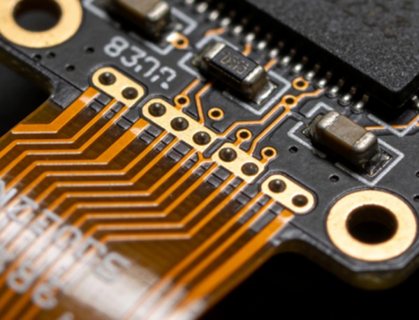
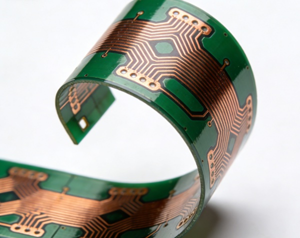
Mechanical reliability is one of the most critical and failure-prone aspects of flexible PCB design. Unlike rigid boards, flexible PCBs are subjected to repeated bending, folding, and mechanical stress during assembly and operation.
This article focuses on bend radius and mechanical reliability in flexible PCB design, explaining how improper bend design leads to cracking, trace failure, and early product failure—and how engineers can prevent these issues through disciplined design practices.
🔗 Part of the Flexible PCB Design Series
Flexible PCB Design: Materials, Layout, Reliability, and Manufacturing
Why Bend Radius Is Critical in Flexible PCBs
When a flexible PCB bends, mechanical strain is introduced into:
- Copper traces
- Adhesive layers
- Dielectric films
Copper has limited elongation tolerance. If the bend radius is too small, copper cracks will form—even if the board appears visually intact.
Mechanical reliability failures often appear after assembly or during field use, making them costly to diagnose and fix.
Static vs Dynamic Bending Applications
Static Bending
- Bent once during assembly
- Shape remains fixed during operation
Examples:
- Folded flex inside enclosures
- Connector interconnects
Static applications tolerate smaller bend radii.
Dynamic Bending
- Repeated bending during operation
- High cycle count
Examples:
- Hinges
- Wearables
- Printer heads
Dynamic applications require much larger bend radii and stricter design rules.
Bend Radius Design Guidelines
General Rule-of-Thumb
| Application Type | Minimum Bend Radius |
|---|---|
| Static bending | ≥ 6–10 × flex thickness |
| Dynamic bending | ≥ 10–20 × flex thickness |
These are starting points—not guarantees. Material choice and copper structure significantly affect reliability.

Copper Layer Placement and Neutral Axis
The neutral axis is the region within the flex stack where strain is minimized during bending.
Best practices:
- Place copper layers as close as possible to the neutral axis
- Use symmetric copper distribution
- Avoid placing copper at the outermost layers in bend areas
Proper stackup design dramatically improves bend life.
🔗 Related topic:
Flexible PCB Materials and Stackup Design
Copper Thickness and Trace Design in Bend Areas
Copper thickness has a direct impact on mechanical reliability.
Recommendations:
- Use thinner copper (e.g., 0.5 oz or less) in bend regions
- Avoid plated-through vias in dynamic bend areas
- Use curved or teardrop trace shapes
- Route traces perpendicular to the bend axis
Sharp corners and width transitions accelerate crack initiation.
Adhesives, Coverlays, and Mechanical Stress
Adhesive layers and coverlays affect flexibility and stress distribution.
Key considerations:
- Adhesive-less laminates improve reliability
- Coverlay openings should not overlap bend zones
- Avoid stiffeners near bend regions
Material stack decisions strongly influence mechanical fatigue life.
Common Mechanical Failure Modes in Flexible PCBs
Typical flex PCB failures include:
- Copper trace cracking
- Delamination
- Via barrel fracture
- Intermittent electrical opens
These failures often escape initial testing and appear later in the product lifecycle.
Design for Assembly and Mechanical Constraints
Mechanical reliability must account for real-world assembly conditions.
Designers should consider:
- Actual bend angles during installation
- Assembly tooling constraints
- Strain introduced by connectors and stiffeners
Close collaboration with mechanical engineers is essential.
Testing and Validation for Flex Reliability
Validation methods include:
- Bend cycle testing
- Dynamic flex testing
- Cross-section analysis
Testing should reflect actual use conditions rather than ideal assumptions.
Best Practices Summary
To improve mechanical reliability in flexible PCB design:
- Define static vs dynamic bending early
- Use conservative bend radius values
- Optimize stackup around the neutral axis
- Minimize copper thickness in bend zones
- Validate with realistic mechanical testing
Conclusion
Bend radius design is a primary determinant of flexible PCB reliability. By understanding mechanical stress mechanisms and applying disciplined design rules, engineers can significantly reduce flex PCB failures and extend product lifetime.
This article establishes the mechanical reliability foundation for flexible PCB design.
FAQ – Bend Radius & Flex PCB Reliability
A: Copper traces may crack, leading to intermittent or permanent open circuits.
A: Both are critical. Material choice and stackup determine how much strain copper experiences during bending.
A: Vias should be avoided in dynamic bend areas whenever possible.
A: Thickness includes all dielectric layers, copper, adhesives, and coverlays.
A: Mechanical fatigue accumulates over repeated bend cycles, eventually causing cracks.
A: Yes. Curved routing reduces stress concentration and improves reliability.