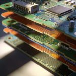
In multilayer PCB design, the stackup defines how copper layers and dielectric materials are arranged inside the board. A well-designed stackup helps maintain signal integrity, supports controlled impedance routing, and ensures mechanical stability during manufacturing and assembly.
FR4 materials are widely used in multilayer boards because they provide a balance between electrical performance and manufacturing cost.
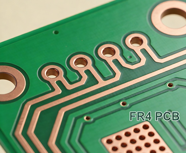
Before designing a stackup, it is useful to understand the properties of FR4 laminates. More details can be found in FR4 PCB Material Guide: Properties, Advantages, and Applications.
What Is a PCB Stackup?
A PCB stackup describes the vertical structure of the board. It includes the number of copper layers, the thickness of dielectric materials, and the arrangement of signal and reference planes.
Typical elements of a stackup include:
- copper signal layers
- power planes
- ground planes
- core materials
- prepreg layers
Together, these layers determine the electrical and mechanical behavior of the PCB.
The total board thickness also depends on the stackup configuration. Common thickness standards are explained in FR4 PCB Thickness Guide: 0.8mm vs 1.0mm vs 1.6mm Explained.
Basic FR4 PCB Stackup Structures
Multilayer FR4 boards are usually designed with symmetric stackups to reduce mechanical stress during fabrication.
Several stackup configurations are commonly used.
4-Layer Stackup
A 4-layer PCB is one of the most widely used multilayer structures.
Typical configuration:
- Layer 1: Signal
- Layer 2: Ground plane
- Layer 3: Power plane
- Layer 4: Signal
This structure allows signal layers to reference a stable ground plane, which improves signal integrity and reduces electromagnetic interference.
4-layer boards are commonly used in embedded systems, industrial controllers, and communication devices.
6-Layer Stackup
A 6-layer stackup provides additional routing capacity and improved signal control.
Example structure:
- Layer 1: Signal
- Layer 2: Ground
- Layer 3: Signal
- Layer 4: Signal
- Layer 5: Power
- Layer 6: Signal
Additional layers allow designers to separate high-speed signals from power distribution networks.
8-Layer Stackup
8-layer boards are often used in high-performance electronics such as networking equipment and advanced computing systems.
A common configuration includes dedicated ground and power planes surrounding signal layers.
Example structure:
- Signal
- Ground
- Signal
- Power
- Power
- Signal
- Ground
- Signal
This arrangement improves electromagnetic shielding and supports more controlled impedance routing.
Design considerations for high-speed circuits are discussed further in High-Speed PCB Design Guide.
How to Design an FR4 PCB Stackup
Designing an FR4 PCB stackup usually begins during the early stages of PCB layout planning. The goal is to create a balanced layer structure that supports signal routing, power distribution, and impedance control.
A typical stackup design process includes the following steps.
- 1. Define the Layer Count
The first step is determining how many layers the board requires.
2-layer boards are common for simple circuits
4-layer boards are widely used for embedded systems
6-layer or 8-layer boards are often required for high-speed designs
The layer count depends mainly on routing density and signal integrity requirements. - 2. Assign Signal and Reference Planes
Once the layer count is defined, the next step is assigning signal layers and reference planes.
A common practice is placing signal layers next to solid ground planes. This provides a stable return path for high-speed signals and helps reduce electromagnetic interference.
For example, a typical 4-layer structure may include:
Top layer — signal routing
Inner layer — ground plane
Inner layer — power plane
Bottom layer — signal routing - 3. Determine Dielectric Thickness
Dielectric thickness between layers affects both impedance and mechanical thickness.
Manufacturers usually provide standard core and prepreg materials with specific thickness options. Designers often select combinations that achieve the target board thickness while maintaining proper signal spacing.
Standard PCB thickness options are discussed in FR4 PCB Thickness Guide: 0.8mm vs 1.0mm vs 1.6mm Explained. - 4. Calculate Controlled Impedance
For high-speed signals such as DDR, PCIe, or high-speed communication buses, controlled impedance is required.
Impedance calculations depend on:
trace width
copper thickness
dielectric constant
distance to reference plane
Many PCB manufacturers provide impedance calculators or stackup design services to help engineers define these parameters. - 5. Balance the Stackup
A balanced stackup helps prevent board warping during lamination and soldering processes.
To maintain balance:
copper layers should be distributed symmetrically
dielectric thickness above and below the center should be similar
large copper planes should be evenly placed
These practices improve both manufacturing yield and long-term reliability. - 6. Confirm the Stackup with the PCB Manufacturer
Before finalizing the design, it is important to verify the stackup with the PCB manufacturer.
Manufacturers can confirm:
available laminate materials
prepreg combinations
impedance feasibility
overall board thickness
Working with manufacturer-approved stackups helps avoid fabrication issues later in the production process.
Impedance Control in FR4 PCBs
Controlled impedance is important for high-speed digital and RF circuits. Signal traces must maintain a consistent impedance to avoid reflections and signal degradation.
Impedance depends on several factors:
- trace width
- copper thickness
- dielectric constant of FR4
- distance between signal layer and reference plane
FR4 materials typically have a dielectric constant around 4.2–4.6, although the exact value may vary depending on the manufacturer and frequency.
When designing high-speed PCBs, engineers often work closely with PCB manufacturers to define stackup parameters that meet the required impedance targets.
Dielectric Spacing and Layer Balance
The spacing between copper layers affects both impedance control and electromagnetic performance.
Designers generally follow these principles:
- maintain symmetric stackups
- keep signal layers close to reference planes
- avoid large dielectric thickness variations
- separate high-speed signals from noisy power layers
Balanced stackups help prevent board warping during lamination and reflow processes.
More details about PCB fabrication steps can be found in PCB Manufacturing Process Step by Step.
Stackup Design and Thermal Performance
Although FR4 materials have relatively low thermal conductivity compared with ceramic substrates, stackup structure can still influence heat spreading.
Copper planes inside the PCB can help distribute heat across the board surface.
Thermal design techniques are explained further in Thermal Management in PCB Design.
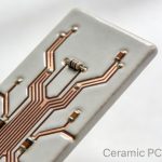
For applications requiring higher thermal performance, alternative substrates such as ceramic boards may be considered. A comparison can be found in Ceramic PCB vs FR4 PCB: Thermal, Electrical, and Cost Comparison.
Working with PCB Manufacturers
Stackup design is usually finalized in collaboration with the PCB manufacturer.
Manufacturers provide stackup tables that define:
- available core thicknesses
- prepreg materials
- copper foil options
- impedance calculation data
Using manufacturer-recommended stackups helps ensure that the board can be produced reliably.
Conclusion
FR4 PCB stackup design plays an important role in determining electrical performance, mechanical stability, and manufacturing reliability.
By carefully arranging signal layers, reference planes, and dielectric materials, engineers can create multilayer boards that support controlled impedance routing and stable signal transmission.
Understanding these stackup principles is essential when designing modern high-speed electronic systems.
FAQ
A: A PCB stackup defines the arrangement of copper layers and dielectric materials inside a multilayer circuit board.
A: Stackup structure affects signal integrity, impedance control, electromagnetic interference, and mechanical stability.
A: A 4-layer stackup with signal, ground, power, and signal layers is one of the most widely used configurations.
A: Trace width, dielectric thickness, copper thickness, and the dielectric constant of FR4 materials all influence impedance.
A: Yes. Balanced stackups and manufacturer-approved layer structures help ensure reliable PCB fabrication and reduce warpage.