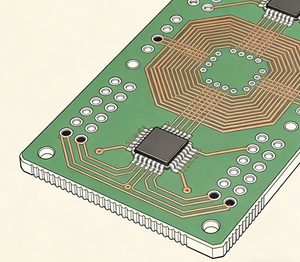
FR4 is the most commonly used substrate material for printed circuit boards. In addition to material properties, the thickness of the PCB also plays an important role in mechanical strength, assembly compatibility, and product design.
Although manufacturers can produce boards in many different thicknesses, several standard values have become common across the industry. Among these, 0.8 mm, 1.0 mm, and 1.6 mm are frequently used in consumer electronics and industrial equipment.
Understanding these thickness options helps designers choose the most appropriate board structure for their applications.
For a broader overview of FR4 materials, see FR4 PCB Material Guide: Properties, Advantages, and Applications.
Why PCB Thickness Matters
PCB thickness influences several aspects of circuit board performance and manufacturing.
Mechanical Strength
Thicker boards are generally more rigid and resistant to bending. This is important for products that may experience vibration or mechanical stress during operation.
Connector Compatibility
Some connectors and edge card slots are designed to work with specific PCB thicknesses. Using non-standard thicknesses may cause assembly or fit issues.
Thermal Behavior
Although PCB thickness does not directly determine thermal conductivity, thicker boards may provide slightly better heat spreading through the copper layers.
Thermal design considerations are discussed further in Thermal Management in PCB Design.
Manufacturing Cost
Boards with unusual thicknesses may require special material combinations or fabrication adjustments, which can increase manufacturing costs.
More details about cost factors are explained in PCB Manufacturing Cost Factors.
Common FR4 PCB Thickness Standards
Several FR4 thickness values have become common industry standards.
These standards allow PCB manufacturers to maintain consistent fabrication processes while ensuring compatibility with common electronic components.
1.6 mm FR4 PCBs
A thickness of 1.6 mm is the most widely used PCB thickness.
Many consumer electronics and industrial circuit boards use this thickness because it provides a good balance between mechanical strength and manufacturing cost.
Typical applications include:
- computer motherboards
- power supplies
- industrial control boards
- communication equipment
Because of its popularity, most PCB fabrication processes and assembly equipment are optimized for 1.6 mm boards.
1.0 mm FR4 PCBs
A 1.0 mm PCB thickness is commonly used in applications where space constraints require thinner boards.
This thickness offers moderate rigidity while reducing overall product size.
Typical applications include:
- compact consumer electronics
- embedded control boards
- portable devices
Although thinner than standard boards, 1.0 mm PCBs still provide sufficient mechanical stability for many products.
0.8 mm FR4 PCBs
A thickness of 0.8 mm is often used in compact electronic products that require lightweight and space-efficient designs.
Common applications include:
- mobile electronics
- IoT devices
- small control modules
- compact LED drivers
Because thinner boards are more flexible, designers may need to consider mechanical reinforcement or mounting strategies.
Other FR4 Thickness Options
In addition to the common thicknesses mentioned above, PCB manufacturers can produce boards in many other sizes.
Examples include:
- 0.4 mm
- 0.6 mm
- 2.0 mm
- 2.4 mm
Very thin boards are often used in space-constrained devices, while thicker boards may be used in applications requiring extra mechanical strength.
When selecting non-standard thicknesses, it is important to confirm manufacturing capabilities with the PCB supplier.
Manufacturing processes for FR4 boards are explained in PCB Manufacturing Process Step by Step.
How PCB Thickness Affects Stackup Design
PCB thickness is closely related to the internal layer structure of the board.
For multilayer boards, the final thickness depends on:
- number of copper layers
- prepreg thickness
- core material thickness
- copper foil weight
Designers must balance electrical performance, impedance control, and mechanical requirements when defining the layer stack.
Additional design considerations can be found in FR4 PCB Stackup Design Guide.
Choosing the Right PCB Thickness
The most appropriate PCB thickness depends on several factors.
Engineers typically consider:
- mechanical strength requirements
- available space in the product enclosure
- connector compatibility
- manufacturing cost
- multilayer stackup requirements
For many general electronics products, 1.6 mm remains the most practical choice. However, thinner boards may be preferred in compact or lightweight designs.
Conclusion
FR4 PCB thickness plays an important role in mechanical stability, product integration, and manufacturing compatibility.
While many thickness options are available, 1.6 mm, 1.0 mm, and 0.8 mm are among the most commonly used standards in electronic products.
By understanding these thickness options and their design implications, engineers can make more informed decisions during the PCB design process.
FAQ
A: The most common standard thickness is 1.6 mm, which is widely used in consumer electronics and industrial circuit boards.
A: A 1.0 mm board is often used in compact devices where reducing product thickness is important.
A: Not necessarily, but thinner boards may be more flexible and require proper mechanical support.
A: Yes. PCB thickness influences layer spacing and impedance control, which can affect signal integrity in high-speed circuits.
A: Yes. Most PCB manufacturers can produce custom thicknesses by adjusting core materials and prepreg layers.