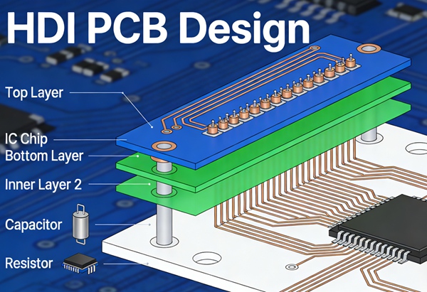
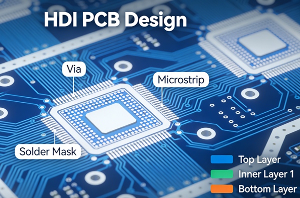
Vias are the foundation of HDI PCB technology. Unlike conventional through-hole vias, HDI PCBs rely on microvias, blind vias, and buried vias to achieve ultra-high routing density, improved signal integrity, and compact board layouts.
This article explains how to design microvias, blind vias, and buried vias in HDI PCBs, including design rules, reliability considerations, and manufacturing constraints.
🔗 Part of the HDI PCB Design Series
HDI PCB Design: Technology, Stackup, Routing, and Manufacturing
What Are Microvias?
Microvias are laser-drilled vias, typically:
- Diameter ≤ 150 μm
- Depth ≤ 1 layer
- Used to connect adjacent layers
They dramatically reduce via parasitics and free routing space.
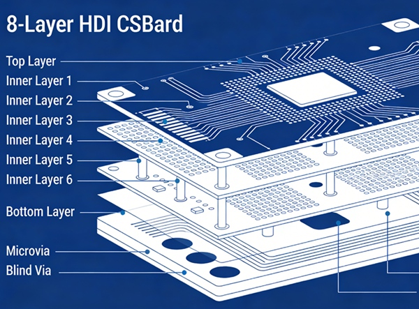
Blind Vias and Buried Vias Explained
Blind Vias
- Connect outer layers to inner layers
- Do not pass through the entire board
Buried Vias
- Connect inner layers only
- Invisible from the surface
Both are created using sequential lamination.
Why HDI Designs Depend on Microvias
Microvias enable:
- Fine-pitch BGA fanout
- Reduced via stubs
- Better high-speed signal integrity
- Smaller board size
For BGA pitches ≤ 0.8 mm, microvias are often mandatory.
Microvia Design Rules and Best Practices
Aspect Ratio Guidelines
- Recommended microvia aspect ratio ≤ 1:1
- Shallower vias improve plating reliability
Stacked vs Staggered Microvias
Stacked Microvias
- Higher density
- Higher cost and reliability risk
Staggered Microvias
- Better reliability
- Preferred for most designs
Staggered microvias are generally recommended unless density demands stacking.
Via-in-Pad Design
Via-in-pad is common in HDI designs but requires:
- Copper filling
- Proper planarization
- Tight process control
Poor via filling leads to solder voids and reliability issues.
Electrical Performance Considerations
HDI via structures reduce:
- Parasitic inductance
- Signal reflection
- Crosstalk
However, poor via geometry can negate these benefits.
Best practices:
- Minimize via count
- Keep via transitions short
- Avoid unnecessary stacked structures
Reliability Risks in HDI Via Structures
Common failure modes include:
- Copper cracking in stacked microvias
- Incomplete via fill
- Delamination during thermal cycling
Reliability risk increases with:
- Excessive stacking
- High aspect ratios
- Poor material selection
Manufacturing Constraints and DFM Rules
HDI via design must align with fabricator capability.
Key DFM considerations:
- Minimum laser via diameter
- Maximum stacking levels
- Via fill material selection
- Registration accuracy
Early DFM review is essential for yield.
🔗 Manufacturing context:
HDI PCB Manufacturing Process and Yield Optimization
When to Use Blind/Buried Vias Instead of Through Vias
Choose blind/buried vias when:
- Routing density is constrained
- Signal integrity is critical
- Board size must be minimized
Through vias remain suitable for low-density areas.
Best Practices Summary
To design reliable HDI vias:
- Use microvias with aspect ratio ≤ 1:1
- Prefer staggered over stacked microvias
- Apply via-in-pad only with proper filling
- Minimize via transitions
- Align designs with manufacturer capability
Conclusion
Microvias, blind vias, and buried vias are the backbone of HDI PCB design. Proper via structure selection and disciplined design practices are essential to achieve high density, good signal integrity, and long-term reliability.
This article forms the technical core of the HDI PCB Design cluster.
FAQ – HDI Microvias and Via Design
A: A microvia is a type of blind via created by laser drilling, typically connecting only adjacent layers.
A: They can be reliable if manufactured correctly, but they carry higher risk than staggered microvias.
A: Via-in-pad is used for fine-pitch BGAs where escape routing space is limited.
A: No. Through vias are still useful for power, ground, and low-density regions.
A: Most manufacturers recommend limiting stacks to 2 levels for reliability.
A: Yes. Shorter via length reduces parasitic inductance and reflections.