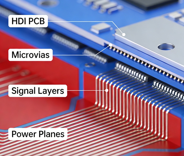
In the world of 5G, AI, and wearable tech, space is the most expensive commodity on a circuit board. Standard through-hole technology often falls short when dealing with fine-pitch BGA components (0.4mm or less). This is where HDI (High-Density Interconnect) technology becomes essential.
At Hansphere, we specialize in the complex buildup processes required to produce reliable HDI boards. It isn’t just about smaller holes; it’s about a fundamental shift in how layers are connected.
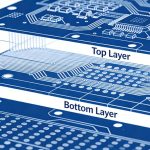
What Is an HDI PCB?
An HDI PCB is characterized by:
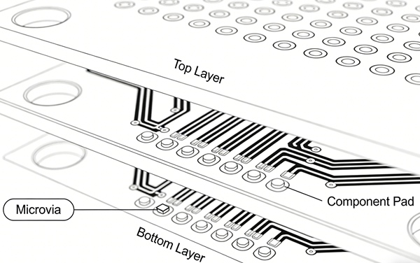
- Microvias (laser-drilled vias ≤150 µm)
- Blind and buried vias
- Fine line / fine spacing routing
- Sequential lamination processes
HDI technology increases interconnection density without increasing board size.
1. The Core Components of HDI Architecture
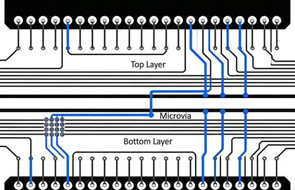
The defining feature of an HDI board is the use of Microvias—laser-drilled holes typically less than 150µm in diameter.
Key Via Structures:
ELIC (Every Layer Interconnect): The pinnacle of HDI, where all layers are connected via copper-filled microvias, allowing for maximum design flexibility.
Blind Vias: Connect an outer layer to at least one inner layer but do not pass through the entire board.
Buried Vias: Connect two or more inner layers without ever reaching an outer surface.
Stacked vs. Staggered Vias: In ultra-dense designs, microvias can be stacked directly on top of each other (filled with copper) or staggered across layers to save space and improve routing.
2. Why Choose HDI? Beyond Just Size
While miniaturization is the obvious benefit, HDI-PCB technology offers significant electrical advantages:
Improved RFI/EMI: Shorter connection paths and better ground plane integrity lead to superior electromagnetic performance.
Reduced Parasitic Capacitance: Smaller vias have less parasitic effect, which is critical for High-Speed PCB Design.
Elimination of Stubs: Unlike through-holes, microvias do not create “stubs” that cause signal reflections.
5 Steps to Transition from Standard to HDI Design
Target: Hardware Engineers & PCB Layout Specialists
Focus: Mastering Microvia Strategy
- Step 1: Analyze BGA Pitch and Fan-out
If your BGA pitch is $\le 0.5mm$, standard via-in-pad is no longer an option. You must move to microvia-in-pad technology to manage the escape routing.
- Step 2: Select the Proper Buildup (e.g., 1+N+1)
Define the number of laser-drilled layers. A “1+N+1” structure means one layer of microvias on each side of a conventional core. For more complexity, move to 2+N+2 or ELIC.
- Step 3: Material Compatibility for Laser Drilling
Not all FR-4 materials are suitable for laser ablation. Choose “Laser-Drillable” prepregs with consistent resin content to ensure clean via holes and reliable plating.
Related: See our High-Speed PCB Material Selection for laminate ideas. - Step 4: Manage Aspect Ratio
To ensure reliable copper plating, the aspect ratio (depth to diameter) of a microvia should ideally be $0.75:1$ or $1:1$. Exceeding this makes chemical fluid exchange difficult during PCB Manufacturing.
- Step 5: Coordinate with Hansphere DFM
HDI fabrication requires precise sequential lamination cycles. Contact our team to verify your stackup and ensure that the via-filling process (VIPPO – Via In Pad Plated Over) aligns with our production standards.
3. Manufacturing Challenges in HDI
Via Filling: Stacked vias must be completely filled with conductive or non-conductive epoxy and plated over to ensure a flat surface for PCB Assembly.
Sequential Lamination: Each HDI layer requires a separate lamination, drilling, and plating cycle. This increases both cost and lead time, making DFM accuracy vital.
Registration Accuracy: Aligning a 100µm laser drill to a 200µm pad across multiple layers requires sub-micron precision.
FAQ – HDI PCB Design Overview
A: HDI stands for High Density Interconnect, referring to PCB designs using microvias and fine routing to increase density.
A: No. HDI is widely used in medical, automotive, and industrial systems.
A: Often yes, but the primary benefit is routing density, not size alone.
A: Upfront cost is higher, but system-level cost may be reduced.
A: We typically support microvias down to 0.1mm (4 mil) for standard production, with advanced capabilities reaching 0.075mm for specialized Flexible PCB or medical applications.
A: While the price per square inch is higher, HDI can actually reduce total system cost. By reducing layer counts (e.g., turning a 14-layer standard board into an 8-layer HDI board), you can often offset the fabrication cost.
A: Yes, but thermal management is key. Using copper-filled microvias can actually improve thermal conductivity away from hot components like high-speed processors.
Conclusion
HDI technology is the bridge to the future of electronics. By mastering microvia structures and sequential lamination, engineers can pack more functionality into smaller, faster, and more reliable devices.
Ready to Level Up Your Design? Hansphere is a leader in HDI fabrication, from 1+N+1 to complex Every-Layer boards. Get an HDI Design Review today or learn more about our advanced equipment on our About Page.