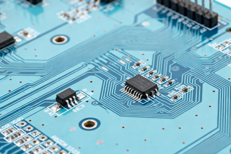
In our previous articles, we’ve explored the essentials of PCB design and how to choose the right PCB design software. Whether you’re a beginner starting out or an experienced designer looking to refine your skills, the journey from conceptualizing your design to finalizing your PCB can be complex. In this article, we will guide you through advanced PCB design techniques, troubleshooting tips, and best practices that will ensure your designs are efficient, manufacturable, and meet the necessary quality standards.
If you haven’t read the first two articles yet, be sure to check them out:
- What is PCB Design? — Understanding the basics of PCB design and its importance in electronics.
- How to Choose the Right PCB Design Software — A guide to help you select the right tools for your PCB design projects.
Now that you understand the fundamental concepts of PCB design and have selected the right software, let’s dive deeper into advanced design techniques, troubleshooting, and best practices to take your designs to the next level.

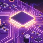
1. Advanced PCB Design Techniques for High-Performance Boards
While understanding the basics of PCB design is essential, there are several advanced techniques that can significantly improve the performance, reliability, and manufacturability of your PCBs. Here are some techniques you should be familiar with:
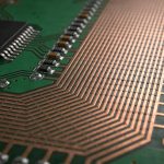
a. High-Speed PCB Design
High-speed designs require careful attention to the integrity of signals as they travel through the board. Signal integrity problems can cause system malfunctions, and in critical applications, even a slight degradation in signal quality can be disastrous.
- Controlled Impedance: High-speed signals need controlled impedance to ensure that they propagate without distortion. Pay attention to the width of your traces and the distance between them to maintain impedance.
- Differential Pair Routing: When routing differential pairs, ensure that the two traces are of equal length and placed closely together to preserve the differential signal.
- Minimizing Crosstalk: To reduce crosstalk (interference between traces), use ground planes to shield sensitive signal traces and maintain proper spacing between high-frequency traces.
b. Power Distribution and Noise Management
A stable and noise-free power supply is crucial for the performance of your PCB. Proper power distribution helps maintain voltage levels and ensures the stability of signals throughout the board.
- Power Plane Design: For multi-layer PCBs, use dedicated power planes to supply consistent voltage and minimize noise. A solid ground plane is essential for grounding.
- Decoupling Capacitors: Decoupling capacitors placed near power pins help to smooth out voltage fluctuations and reduce high-frequency noise.
- Power Integrity: Ensure that the power integrity of your design is carefully analyzed. Tools like PDN (Power Distribution Network) analysis help to check if your power network is optimized and stable.
c. Thermal Management
Heat is one of the most common causes of PCB failure. Components, especially high-power ones, can generate significant heat, which can damage sensitive areas on the board. Good thermal management is key to creating a reliable PCB.
- Thermal Vias and Copper Pour: Use thermal vias to direct heat away from hot components. A copper pour or solid ground plane can help to distribute heat evenly across the PCB.
- Heat Sinks: Consider adding external heat sinks or thermal spreaders to components that generate a significant amount of heat. This helps prevent overheating and improves component longevity.
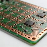
d. Design for Manufacturability (DFM) and Assembly (DFA)
A PCB design should not only be functional but also easy and cost-effective to manufacture and assemble. Implementing DFM (Design for Manufacturability) and DFA (Design for Assembly) practices can reduce production costs and avoid errors during the manufacturing process.
- Standardized Components: Use standardized components to make sourcing easier and more affordable. This also simplifies assembly as components will be more readily available.
- Simplified Routing: Minimize the number of vias and complex routing to simplify the manufacturing process. The more complex your design, the more likely it is to introduce issues during fabrication.
- Keep Trace Widths and Spacing Correct: Ensure that your trace widths and spacing are compatible with the manufacturing capabilities of your chosen PCB fabricator. This will prevent production delays and defects.
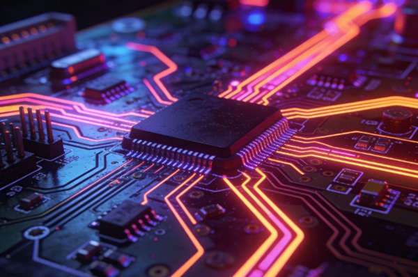
2. PCB Troubleshooting Tips: Common Issues and Solutions
Even with the most careful design, issues can arise during the manufacturing process or when testing your PCB. Here are some common problems and how to resolve them:
a. Signal Integrity Issues
If your PCB isn’t functioning as expected, signal integrity issues could be the cause. These problems can manifest as signal reflections, noise, or reduced performance at high frequencies.
Solution:
- Use impedance-controlled traces and minimize the number of vias.
- Keep traces as short and direct as possible to reduce signal loss.
- Use differential pair routing and ensure that the pair lengths are matched.
b. Overheating Components
When components are overheating, they can cause long-term damage to the PCB and lead to failures.
Solution:
- Ensure thermal vias and copper pours are correctly used to dissipate heat.
- Add heat sinks to components that generate high amounts of heat.
- Use thermal analysis tools in your PCB design software to predict potential hotspots.
c. Design Rule Violations
A common issue in PCB design is violating design rules, such as incorrect trace widths, clearance violations, or via sizes that don’t comply with the manufacturing process.
Solution:
- Use the Design Rule Check (DRC) tool available in your PCB design software to catch violations early.
- Ensure that your design meets the manufacturer’s fabrication capabilities, particularly with regard to trace widths, via sizes, and layer count.
3. Best Practices for Efficient PCB Design
Following best practices can significantly reduce the time spent troubleshooting and revising your PCB design. Here are some tips for optimizing your PCB design process:
a. Plan the Layout Early
Before jumping into placing components, take the time to plan your PCB layout carefully. Consider:
- Component Grouping: Group components logically (e.g., power components together, signal components together) to minimize routing complexity.
- Trace Routing: Plan out your trace routing to minimize the number of vias and to ensure that high-speed signals are properly routed.
b. Use Layered Designs
For complex designs, using multiple layers can help route signals efficiently and maintain power integrity. Design with a layer stack-up that is optimized for both manufacturability and performance.
c. Run DRC Checks Frequently
Throughout the design process, run Design Rule Checks (DRC) frequently to catch violations early. This will help avoid costly mistakes later on.
PCB Design FAQ
A: The best software for advanced PCB design depends on the complexity of your project. For high-end, professional designs, tools like Altium Designer, Cadence Allegro, and Mentor Graphics are excellent. For smaller or less complex projects, tools like KiCad or Autodesk Eagle may be more than sufficient.
A: To prevent overheating, use thermal vias to direct heat away from components, add heat sinks or spreaders to heat-sensitive areas, and ensure that your PCB has an effective copper pour for better heat dissipation.
A: Design for Manufacturability (DFM) refers to designing PCBs in a way that ensures they can be easily and cost-effectively manufactured. This includes considering trace widths, component placement, and reducing the number of vias or complex routing.
A: Signal Integrity is essential for ensuring that high-speed signals maintain their quality throughout the PCB without distortion. Issues like crosstalk, noise, and reflections can lead to functional problems, especially in high-performance designs.
A: To handle PDN design, use decoupling capacitors to stabilize voltage levels, ensure that your power planes are well-designed to avoid noise, and analyze the PDN using specialized software tools to ensure stable power delivery.
Conclusion
In this article, we’ve covered the advanced techniques, troubleshooting tips, and best practices that will help you create high-performance, reliable, and manufacturable PCBs. With the right PCB design software and by following these guidelines, you’ll be able to streamline your design process, avoid common pitfalls, and produce quality PCBs that meet your requirements.
For more detailed information on the fundamentals of PCB design or to choose the right design software, make sure to revisit our previous articles:
By mastering these advanced techniques and adhering to best practices, your PCB design skills will reach new heights, enabling you to tackle more complex projects with confidence.