Selecting the right EDA (Electronic Design Automation) software is one of the most consequential decisions an engineer makes. It’s not just about drawing lines; it’s about managing complex component libraries, ensuring Signal Integrity (SI), and seamless handoff to a PCB Manufacturing partner.
In 2026, the landscape has shifted. AI-assisted routing and cloud-based collaboration are now standard features. Here is how to navigate your options.
1. The Heavyweights: Professional-Grade Tools
Altium Designer: The Industry All-Rounder
Altium remains the most popular choice for professional mid-to-high complexity boards. Its unified environment—integrating schematic, layout, and 3D MCAD—is its biggest strength.
- Best For: Fast-paced commercial product development.
- Key Advantage: Exceptional 3D visualization, which is critical for Rigid-Flex PCB designs where mechanical fit is tight.
- Hansphere Tip: Altium’s Output Job files are the “gold standard” for our factory; they minimize communication errors during fabrication.
Cadence Allegro / OrCAD: The High-Speed Specialist
When you are dealing with multi-gigabit interfaces (PCIe Gen6, DDR5), Allegro is the king. Its constraint manager is unparalleled in handling complex timing and impedance rules.
Key Advantage: Robust simulation and power integrity analysis.
Best For: High-speed digital servers, complex HDI-PCB, and RF systems.
2. Open-Source & Budget-Friendly Options
KiCad: The Community Favorite
KiCad has evolved into a formidable tool that even professional teams are adopting. Since it’s open-source, there are no licensing headaches for startups or hobbyists.
- Best For: Prototyping, IoT devices, and cost-sensitive projects.
- Advantage: Vast community-driven libraries and no subscription fees.
- Pro Tip: If you use KiCad, always double-check your PCB Assembly pick-and-place files, as library footprint origins can sometimes vary.

Autodesk Fusion 360 (formerly EAGLE)
Fusion 360’s biggest draw is its integration with mechanical CAD. If your PCB has a complex housing, the bidirectional syncing is a lifesaver.

4 Steps to Evaluate PCB Software
- Step 1: Assess Project Complexity
Simple (2-4 layers): KiCad or EasyEDA.
Complex (6+ layers, High-speed): Altium or Allegro.
Space-constrained: Look for tools with advanced Flexible PCB support. - Step 2: Check Library & Component Management
Does the tool connect to real-time supply chain data? Ensuring parts are “In Stock” during the design phase is vital for timely PCB Design completion.
- Step 3: Evaluate the Simulation Suite
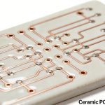
Do you need SPICE simulation or Thermal analysis? If your board uses Ceramic PCBs for high-power LEDs, thermal simulation is non-negotiable.
- Step 4: Verify Manufacturer Compatibility
Before committing, ask: Does this tool export ODB++ or standard Gerber X2? These formats ensure your Rigid PCB is built exactly as intended.
3. Comparison Table: Which One Is for You?
| Feature | Altium Designer | Cadence Allegro | KiCad | Fusion 360 |
| Learning Curve | Medium | Steep | Low-Medium | Low |
| High-Speed Design | Excellent | Best-in-class | Good | Fair |
| Collaboration | Excellent (365) | Good | Limited | Excellent |
| Cost | High (Subscription) | High (Enterprise) | Free | Mid-range |
4. Why Software Choice Affects Manufacturing
At Hansphere, we see thousands of designs every year. The most common delays occur because of “Translation Errors”—when software exports files that the manufacturing equipment can’t interpret correctly.
- Pro Tip: Always run a DFM (Design for Manufacturing) check within your software before exporting. If your tool supports it, use the manufacturer’s design rule file (DRC) directly.
PCB Design Tools FAQ
A: It is difficult. While most tools have “importers,” they often lose complex constraints or specific copper pour settings. It’s best to finalize the tool choice at the schematic stage.
A: For non-critical signals on simple boards, yes. However, for high-speed paths or High Frequency PCBs, manual routing is still required to ensure signal integrity.
A: We prefer ODB++ or IPC-2581 as they contain more intelligence than standard Gerbers, reducing the risk of layer misalignment.
Conclusion
There is no “perfect” tool—only the right tool for your specific engineering and budget requirements. Whether you choose the power of Allegro or the flexibility of KiCad, your focus should always be on Design for Excellence (DFX).
Need a Professional Design Review? Our engineering team at Hansphere is proficient in all major EDA tools. We can help you optimize your layout for better yield and lower costs. Get a Quote Today.