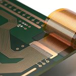
Rigid-flex PCBs combine rigid circuit boards with flexible interconnects in a single structure. The stackup determines how these materials interact during manufacturing and how the board behaves mechanically during operation.
A poorly designed stackup can lead to delamination, copper cracking, or reduced manufacturing yield. For this reason, stackup planning should be one of the earliest steps in rigid-flex PCB design.
If you are new to this technology, you may first want to review the fundamentals explained in Rigid-Flex PCB Design: Fundamentals and Applications.
Understanding Rigid-Flex PCB Stackups
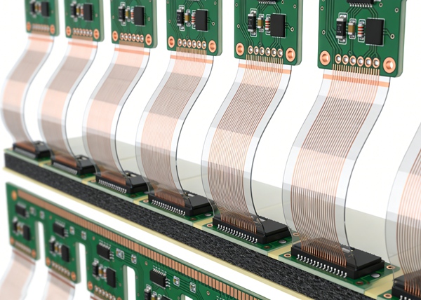
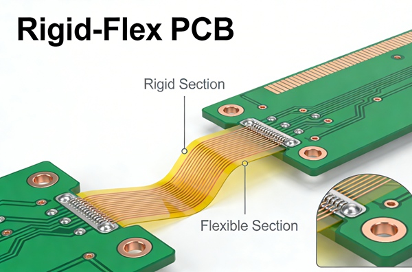
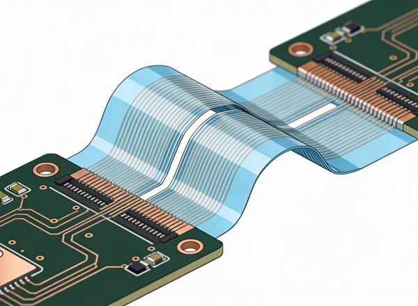
A rigid-flex PCB stackup typically includes both rigid laminate layers and flexible polyimide layers within the same board.
The rigid sections provide mechanical stability and component mounting areas, while the flex sections allow the board to bend or fold during installation.
The basic structure includes:
- Rigid FR-4 layers for component placement
- Flexible polyimide substrates
- Adhesive or adhesive-less bonding layers
- Copper circuitry layers
- Coverlay protection on flex sections
The stackup must be carefully balanced so that stress during bending is distributed evenly across the flex layers.
For an overview of rigid-flex technology and its typical applications, see Rigid-Flex PCB Design: Fundamentals and Applications.
Common Rigid-Flex Stackup Structures
Rigid-flex PCBs can be built in many configurations depending on the application.
Single Flex Layer Stackup
The simplest configuration uses a single flexible layer connecting two rigid sections. This design is commonly used in compact consumer electronics and wearable devices.
Advantages include lower cost and simpler manufacturing, but routing density is limited.
Double Flex Layer Stackup
A more advanced design includes two flexible copper layers separated by polyimide dielectric. This allows controlled impedance routing and higher signal density.
Double-layer flex stackups are frequently used in medical devices, cameras, and aerospace systems.
Multilayer Rigid-Flex Stackup
High-performance electronics may use multilayer rigid-flex stackups with multiple rigid layers and embedded flex circuits.
These designs support high-speed signals, dense component placement, and complex routing requirements.
However, multilayer rigid-flex boards require careful lamination planning and close collaboration with the PCB manufacturer.
A deeper discussion of manufacturing considerations is covered in Rigid-Flex PCB Manufacturing Process and Design Guidelines.
Material Selection for Rigid-Flex Stackups
Material selection has a direct impact on reliability and mechanical performance.
The most common materials include:
Rigid Materials
Rigid sections typically use FR-4 laminates, similar to conventional PCBs. High-temperature variants may be required for demanding environments.
Flexible Substrates
Flexible circuits generally use polyimide materials due to their excellent thermal stability and flexibility.
Polyimide also maintains mechanical strength after repeated bending cycles.
Copper Foil Types
Two copper types are commonly used:
Rolled-annealed copper provides superior flexibility and fatigue resistance, making it the preferred option for flex regions.
Electrodeposited copper is cheaper but less resistant to repeated bending.
Because copper properties influence long-term durability, the choice of copper foil should be considered early in the stackup design process.
Designing the Flex Region
The flex region is the most critical part of a rigid-flex PCB.
Design rules for this area include:
Avoid placing vias inside bend regions whenever possible.
Use smooth trace routing instead of sharp angles to reduce stress concentration.
Keep copper distribution balanced across the flex layers.
Maintain adequate spacing between traces to avoid cracking during repeated bending.
Another important factor is the bend radius, which determines how tightly the flex section can bend without damaging the copper.
Detailed reliability guidelines are explained in Rigid-Flex PCB Bend Radius and Reliability Design Rules.
Transition Between Rigid and Flex Areas
The transition zone between rigid and flexible sections is another area where design problems frequently occur.
Abrupt changes in stiffness can create mechanical stress and increase the risk of delamination.
Designers usually implement gradual transitions by tapering copper layers or adjusting dielectric thickness near the rigid-flex boundary.
Manufacturers may also add strain relief structures to reduce mechanical stress.
Manufacturing Considerations
Rigid-flex stackups require more complex manufacturing processes compared with traditional PCBs.
Key considerations include:
Multiple lamination cycles are often required.
Precise alignment is necessary to maintain layer registration between rigid and flexible sections.
Drilling and plating processes must accommodate both rigid and flexible materials.
Close communication with the PCB manufacturer during stackup planning can significantly reduce production issues and improve manufacturing yield.
Conclusion
Rigid-flex PCB stackup design plays a central role in both electrical performance and mechanical reliability.
A well-structured stackup should balance copper layers, select appropriate materials, and carefully define flex regions and rigid transitions.
By considering manufacturing constraints and mechanical behavior early in the design stage, engineers can avoid many common reliability problems associated with rigid-flex circuits.
FAQ
A: A rigid-flex PCB stackup describes how rigid layers, flexible substrates, copper layers, and bonding materials are arranged within a rigid-flex circuit board. The stackup defines the electrical performance, mechanical flexibility, and manufacturability of the board.
A: Rigid-flex stackups usually combine FR-4 laminates for rigid sections with polyimide materials for flexible circuits. Copper foil, adhesives, and protective coverlays are also used to complete the structure.
A: Stackup planning ensures that the board can bend reliably without damaging the copper layers. It also affects signal integrity, thermal performance, and manufacturing yield.
A: Yes. Multilayer rigid-flex stackups can support controlled impedance routing and differential pairs, making them suitable for high-speed digital and RF applications.
A: Rigid-flex PCBs can range from simple two-layer flex designs to complex structures with more than twenty layers. The maximum layer count depends on manufacturing capability and application requirements.