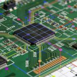
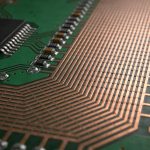
Hansphere provides engineering-driven PCB design services for customers in Saudi Arabia. Our focus is on production-ready PCB design that supports stable manufacturing and reliable assembly, rather than layouts created only to meet basic electrical requirements.
We work with customers from early concept and schematic development through detailed PCB layout, ensuring that design decisions align with manufacturing and assembly constraints from the beginning.

Engineering-Focused PCB Design for Saudi Arabia Projects
PCB design is not only about routing signals. For projects serving the Saudi Arabian market, reliability, documentation, and manufacturability are critical factors.
Hansphere approaches PCB design as a structured engineering process:
- Design decisions are reviewed with manufacturing and assembly in mind
- Potential production risks are identified early
- Documentation is prepared for smooth handover to fabrication and assembly
This approach helps reduce redesign cycles and unexpected delays later in the project.
PCB Design Capabilities
Schematic Design and Review
We support both new schematic development and review of existing designs. Our schematic services include:
- New schematic creation based on functional requirements
- Review of customer-provided schematics
- Electrical rule checks
- Power architecture and interface review
Early schematic review helps ensure that the design is suitable for PCB layout and downstream production.
PCB Layout and Stack-Up Design
Hansphere provides multilayer PCB layout services with attention to signal integrity, power distribution, and manufacturability.
Our layout capabilities include:
- Multilayer PCB layout
- Stack-up definition and layer planning
- Controlled impedance planning
- Component placement optimization
Stack-up and layout decisions are coordinated with manufacturing requirements to avoid late-stage changes.

Signal Integrity and Power Integrity Considerations
For designs involving high-speed signals or sensitive power networks, we apply practical engineering guidelines during layout:
- Controlled routing for high-speed interfaces
- Return path and grounding strategy
- Power plane design and decoupling placement
These considerations help improve electrical performance while maintaining manufacturing feasibility.
Design for Manufacturing and Assembly (DFM & DFA)
Design for Manufacturing (DFM) and Design for Assembly (DFA) are integrated into the PCB design process.
Our DFM and DFA activities include:
- Review of trace widths, spacing, and via structures
- Assessment of component footprints and land patterns
- Assembly clearance and soldering considerations
- Early feedback from fabrication and assembly perspectives
Addressing these factors during design helps minimize rework and production issues.
PCB manufacturing services in Saudi Arabia
PCB assembly services in Saudi Arabia
Design Standards and Documentation
Hansphere follows established industry standards and customer-specific requirements during PCB design, including:
- IPC-2221 and related PCB design standards
- IPC-7351 land pattern guidelines
- Customer-defined electrical and mechanical constraints
Typical design deliverables include:
- Gerber or ODB++ files
- Drill files
- Bill of Materials (BOM)
- Assembly drawings
- Manufacturing notes and documentation
Clear documentation supports smooth transitions to manufacturing and assembly.

How to Start a PCB Design Project in Saudi Arabia
Starting a PCB design project with Hansphere follows a clear and structured process:
- Starting a PCB design project with Hansphere follows a clear and structured process:
- Step 2: Engineering review and design feasibility discussion
- Step 3: PCB layout, DFM/DFA review, and design refinement
- Step 4: Final design documentation for manufacturing and assembly
This process ensures that design intent and production requirements remain aligned.
Saudi Arabia FAQ
A: Yes. We can review and redesign existing PCB layouts to improve manufacturability and assembly reliability.
A: Yes. Hansphere provides independent design reviews and DFM/DFA feedback for third-party PCB designs.
A: Yes. Our PCB design process is closely aligned with manufacturing and assembly requirements to support smooth production.
A: Yes. We support PCB design for prototypes, pilot runs, and small-to-medium production volumes.
Work with Hansphere
Hansphere works with customers in Saudi Arabia as a PCB design partner focused on practical engineering, clear documentation, and production readiness.
Our team supports projects from early concept through final design handover, helping customers move efficiently from design to manufacturing and assembly.


