As Saudi Arabia accelerates its digital transformation under Vision 2030, the demand for localized electronics development and high-quality hardware has reached an all-time high. From NEOM’s smart city infrastructures to the growing industrial automation in Jubail and Yanbu, reliable PCB manufacturing is the backbone of this technological leap.
At Hansphere, we bridge the gap between complex electronic design and physical reality, providing specialized PCB fabrication services tailored to the unique environmental and industrial requirements of the Saudi Arabian market.

Meeting the High Standards of Saudi Arabia’s Electronics Sector
Electronic projects in Saudi Arabia often face extreme environmental conditions, such as high ambient temperatures and dust. Standard PCB fabrication isn’t enough; you need boards built for durability and thermal stability.
Hansphere supports Saudi-based engineers and enterprises with:
- Industrial-Grade Reliability: PCBs designed to withstand the harsh thermal cycles of the Middle East.
- Prototyping to Mass Production: Whether you are a startup in Riyadh or an established manufacturer in Dammam, we scale with your project needs.
- Seamless Logistics: We have optimized our supply chain to ensure smooth customs clearance and fast delivery to major Saudi hubs including Jeddah, Riyadh, and Al Khobar.
Technical Capabilities: Beyond Standard Fabrication
We don’t just manufacture boards; we provide engineering-led solutions. Our facility is equipped to handle the most demanding specifications required by modern IoT, defense, and energy sectors.
Our Core Manufacturing Specs:
- Advanced Layer Count: From simple double-sided boards to complex 32-layer multilayer PCBs.
- High-Density Interconnect (HDI): Supporting 1+N+1 to Any-layer HDI structures for compact consumer electronics and medical devices. Explore our HDI PCB Technology.
- Material Diversity: We stock high-performance materials including High-Tg FR-4 (essential for Saudi’s heat), Rogers, and Polyimide for Rigid-Flex PCB applications.
- Precision Tolerances: 3mil/3mil trace width/spacing for high-speed digital designs.
Why Global Engineers Trust Hansphere
In the PCB industry, “Experience” and “Authority” are proven through quality control. Hansphere adheres to international standards to ensure every board arriving in Saudi Arabia is “Plug-and-Play” ready.
- IPC Class 2 & 3 Compliance: We manufacture according to IPC-A-600 standards, ensuring your boards meet rigorous aerospace or medical reliability.
- Rigorous Testing: Every batch undergoes Automated Optical Inspection (AOI), Flying Probe Testing, and X-ray inspection for BGA-heavy designs.
- DFM Support: Our engineers perform a Design for Manufacturing (DFM) check before production starts, identifying potential yield issues that could delay your Saudi project timelines.
Need a complete solution? Our manufacturing process integrates perfectly with ourPCB Assembly Services in Saudi Arabia, offering a turnkey experience from bare board to finished product.
Localized Support for Saudi Engineers
We understand the challenges of cross-border procurement. To better serve our Saudi clients, we offer:
- Compliance Documentation: Providing all necessary COC (Certificate of Conformity) and material data sheets.
- Technical Consultation: Not sure which stack-up is best for your High-Speed PCB Design? Our experts are available for real-time consultation.
- Fast Quoting: Upload your Gerber files (RS-274X or ODB++) and receive a detailed quote within 24 hours.

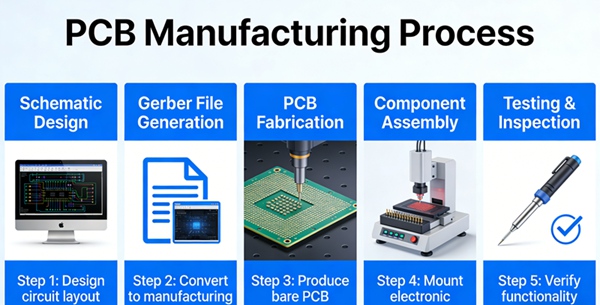
How to Start a PCB Manufacturing Project in Saudi Arabia
PCB manufacturing projects with Hansphere follow a clear and structured process:
- Step 1: Provide Gerber files, ODB++ data, stack-up details, and manufacturing notes
- Step 2: Engineering and manufacturability review
- Step 3: Confirmation of materials, specifications, and production parameters
- Step 4: PCB fabrication and inspection
- Step 5: Delivery or handover to PCB assembly
This process helps ensure transparency and alignment throughout manufacturing.
Frequently Asked Questions (FAQ)
A: Yes, we use premium carriers like DHL and FedEx to ensure fast and secure delivery across the Kingdom, typically within 5-7 business days after fabrication.
A: Absolutely. We recommend High-Tg (170-180°C) or ceramic-based PCBs for Saudi’s outdoor environments to prevent delamination and circuit failure.
A: Yes. Many clients use our PCB Design Services to optimize their layouts specifically for our manufacturing tolerances, ensuring the highest yields.
Start Your Project Today
Whether you are developing the next generation of renewable energy systems or localizing consumer electronics, Hansphere is your trusted partner for PCB manufacturing in Saudi Arabia.
Get a Free Quote Now and let’s bring your Saudi Vision 2030 project to life.