Why ENIG PCB Surface Finish is the Standard for Modern Electronics
When diving into the intricacies of printed circuit board fabrication, one question frequently arises among designers and engineers: why enig pcb surface finishes have become the definitive standard in the modern electronics industry. As devices become smaller, faster, and more reliable, the choice of surface finish is no longer just an afterthought; it is a critical decision that impacts the longevity and functionality of the final product.
Electroless Nickel Immersion Gold, commonly referred to as ENIG, offers a myriad of advantages that cater perfectly to the rigorous demands of contemporary electronic components. From ensuring perfectly flat surfaces for fine-pitch components to providing exceptional oxidation resistance, understanding why enig pcb surface treatments are preferred requires a deep dive into its composition, benefits, and applications.
What is ENIG Surface Finish?
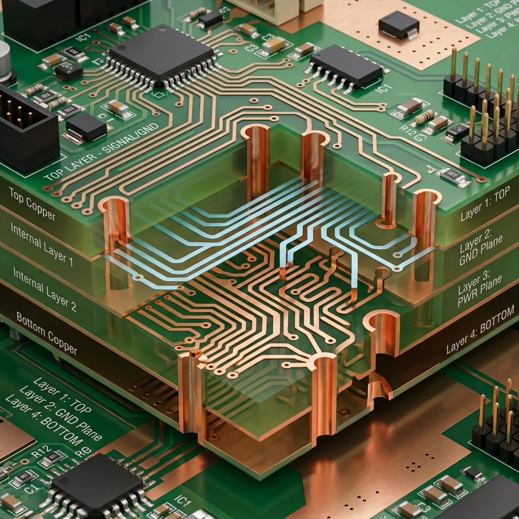
ENIG is a double-layer metallic coating consisting of a thin layer of gold over a thicker layer of electroless nickel. The nickel acts as a barrier to the copper beneath it, preventing it from oxidizing and reacting with other elements, while also serving as the surface to which components are soldered. The thin gold layer protects the nickel during storage and provides the low contact resistance required for certain applications.
Unlike some other surface finishes that may degrade over time or present uneven topographies, ENIG offers a consistent, reliable, and highly functional coating. This consistency is a primary factor in the broader Quy trình sản xuất PCB, where predictability is paramount for high-yield production.
Key Advantages of the ENIG Finish
There are several compelling reasons why the electronics industry has shifted heavily toward this specific coating.
1. Unmatched Surface Planarity
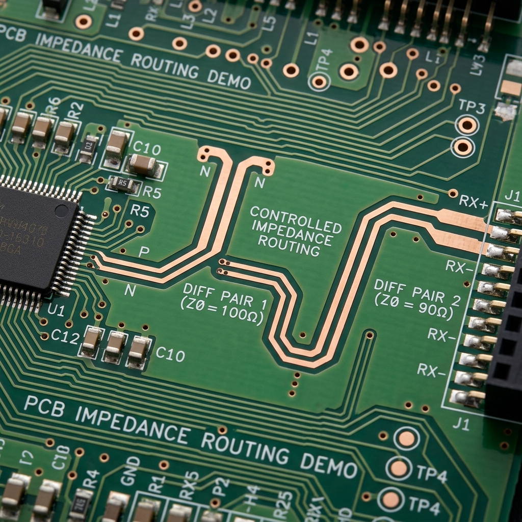
Modern PCBs often feature complex, high-density designs with fine-pitch components such as Ball Grid Arrays (BGAs) and Quad Flat Packages (QFPs). These components require an absolutely flat surface for successful soldering. ENIG provides excellent planarity, reducing the risk of soldering defects compared to finishes like Hot Air Solder Leveling (HASL). If you are curious about the direct comparison, you can read more about HASL vs ENIG.
2. Extended Shelf Life
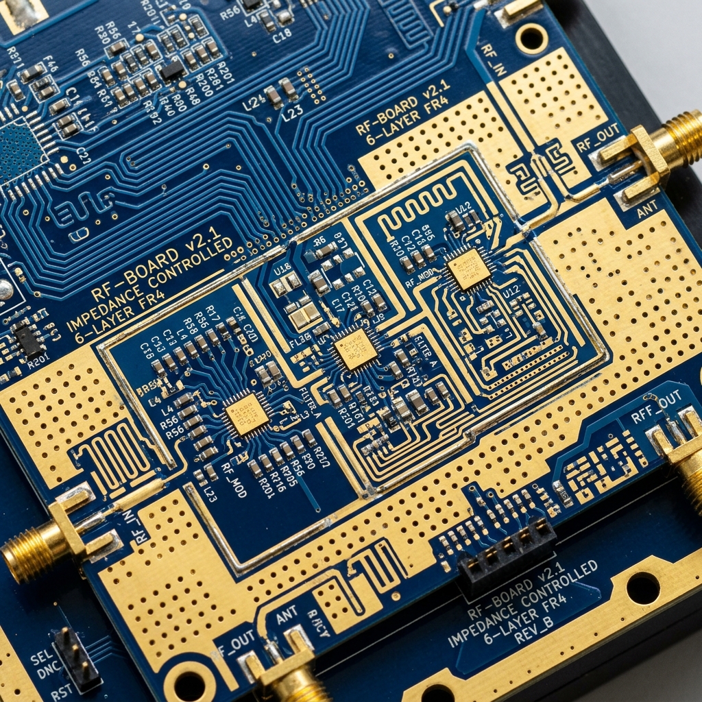
The gold layer in ENIG protects the underlying nickel from oxidation, resulting in a shelf life that typically exceeds 12 months. This extended usability makes it ideal for manufacturers who may need to store boards for significant periods before final Lắp ráp bảng mạch in (PCB) occurs.
3. Lead-Free and RoHS Compliant
As global regulations tighten regarding the use of hazardous substances in electronics, ENIG has emerged as a premier lead-free alternative. It fully complies with the Restriction of Hazardous Substances (RoHS) directives, ensuring your products can be sold in global markets without regulatory hurdles.
4. Excellent Electrical Performance
For high-frequency applications, ENIG is highly favorable. It does not interfere with signal integrity in the same way that thicker, more uneven finishes might. Additionally, it serves excellently for aluminum wire bonding and membrane switches due to its low contact resistance.
How ENIG is Applied to a PCB
The application of an ENIG finish is a complex, multi-step chemical process that requires precise control. Here is a breakdown of the typical steps involved.
Step 1: Cleaning
The copper surface of the PCB must be thoroughly cleaned using acid or alkaline cleaners to remove any oils, fingerprints, or oxidation. This ensures that the subsequent chemical layers bond correctly.
Step 2: Micro-etching
The copper is lightly etched to roughen the surface at a microscopic level. This micro-roughness improves the mechanical adhesion of the chemical layers that will follow.
Step 3: Catalyst Application
A catalyst, usually a palladium-based solution, is applied to the copper. This catalyst initiates the electroless nickel plating process by providing a reactive surface.
Step 4: Electroless Nickel Plating
The board is submerged in a chemical bath containing nickel salts. Through an auto-catalytic reaction, a layer of nickel (typically 3-6 microns thick) is deposited evenly across the exposed copper. This layer forms the solderable surface and the diffusion barrier.
Step 5: Immersion Gold Plating
Finally, the board is immersed in a gold solution. The gold replaces a thin layer of nickel at the surface via a displacement reaction. The gold layer is very thin (usually 0.05-0.1 microns) and serves solely to protect the nickel until soldering.
Các câu hỏi thường gặp
What is “Black Pad” syndrome in ENIG?
Black Pad is a rare but severe defect associated with the ENIG process. It occurs when the nickel layer is over-corroded during the immersion gold deposition step, leading to poor solder joint reliability. It typically manifests as a dark, oxidized nickel surface and can cause components to easily shear off the board.
Is ENIG more expensive than HASL?
Yes, ENIG is generally more expensive than HASL. The higher cost is due to the raw materials (gold) and the complexity of the chemical plating process. However, for high-density, high-reliability boards, the benefits in yield and performance easily outweigh the initial cost difference.
Can ENIG be used for wire bonding?
ENIG is suitable for aluminum wire bonding, but it is typically not recommended for gold wire bonding. For gold wire bonding, a thicker gold layer is required, which is usually achieved through an Electrolytic Hard Gold finish or ENEPIG (Electroless Nickel Electroless Palladium Immersion Gold).