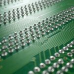
In today’s era where electronic products are ubiquitous, the Printed Circuit Board (PCB) serves as the “skeleton” and “nervous system” of electronic devices, carrying the crucial function of connecting all electronic components. An excellent PCB design not only ensures the proper functionality of the circuit but also enhances product performance, reliability, and manufacturing yield. This article will provide a comprehensive PCB design guide, from fundamentals to advanced techniques, helping you create professional-grade circuit boards.
PCB Design Fundamentals and Core Principles
1.1 Design Process Overview
Successful PCB design follows a systematic process:
- Requirement Analysis and Specification Definition
- Schematic Design and Component Selection
- Component Placement Planning
- Routing Strategy Development
- Design Rule Check (DRC)
- Manufacturing File Output
1.2 Ten Core Design Principles
- Signal Integrity Priority: Minimize high-frequency signal paths, avoid sharp-angle turns
- Power Integrity Management: Reasonably plan power and ground layers
- Thermal Management Consideration: Disperse high-heat components, increase heat dissipation paths
- Electromagnetic Compatibility (EMC): Reduce loop area, use shielding appropriately
- Design for Manufacturability (DFM): Comply with manufacturer capabilities and limitations
- Design for Testability (DFT): Reserve test points and interfaces
- Modular Layout: Group functionally related components together
- Layer Stack-up Optimization: Allocate layer sequence reasonably based on signal types
- Consistent Component Orientation: Facilitates soldering and inspection
- Adequate Safety Spacing: Prevent short circuits and arc discharge
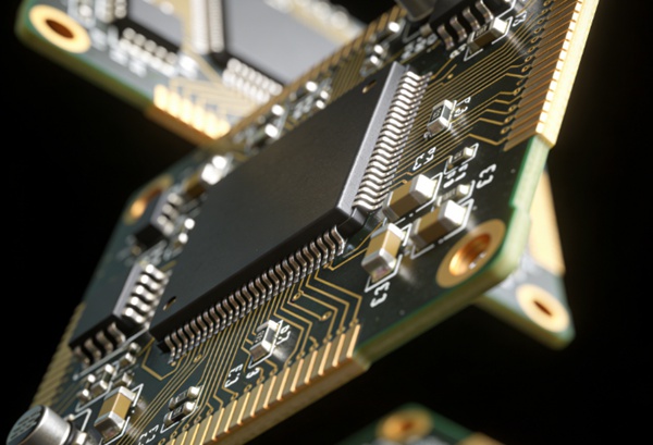
Advanced Layout Strategies and Signal Integrity
2.1 Intelligent Component Placement Techniques
- Functional Partitioning Method: Layout the circuit in zones by function (power, analog, digital, RF)
- Signal Flow Orientation: Place components according to signal flow to reduce crossover and backtracking
- Critical Components First: Place connectors, processors, and other key components first
- Thermal-Sensitive Component Isolation: Keep temperature-sensitive components away from heat sources
2.2 High-Speed Signal Layout Essentials
As signal frequencies increase, PCB design faces new challenges:
- Impedance Control: Precise calculation and implementation of microstrip and stripline
- Differential Pair Routing: Maintain equal length, spacing, and symmetry
- Signal Return Path: Provide the shortest return path for high-speed signals
- Crosstalk Minimization: Reduce interference through spacing, shielding, and layer assignment
2.3 Power Distribution Network (PDN) Design
Efficient PDN design is key to stability:
- Multilayer Board Advantages: Use dedicated power and ground layers
- Decoupling Capacitor Strategy: Optimization of capacitor value combinations and placement
- Power Plane Splitting Techniques: Proper isolation of analog and digital power supplies
- Current Carrying Capacity: Calculate trace width based on current requirements
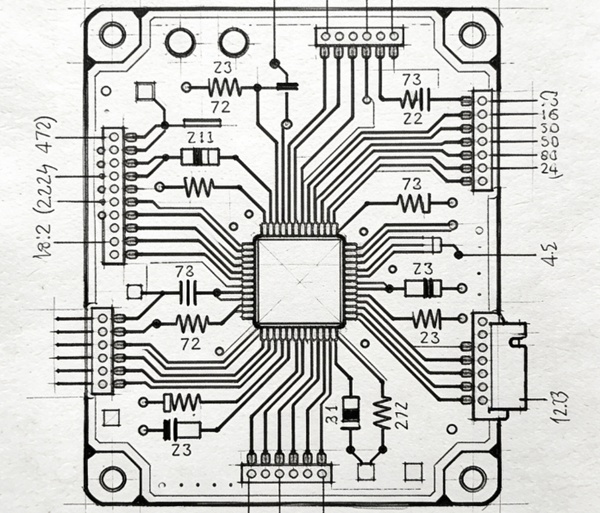
The Art of Routing and Best Practices
3.1 Routing Priority Strategy
- Power Traces: Route power traces first, ensuring sufficient width and low impedance
- Critical Signals: Clocks, differential pairs, high-speed signals
- Sensitive Signals: Analog signals, high-impedance nodes
- General Signals: Low-speed digital signals, control lines
3.2 Advanced Routing Techniques
- Length Matching: Achieve equal length for timing-critical signals using serpentine traces
- Topology Optimization: Appropriate selection of point-to-point, star, or daisy-chain topologies
- Via Management: Reduce via count, optimize via size and placement
- 3D Routing Check: Consider spatial constraints during actual assembly
3.3 Ground System Design
Grounding is one of the most misunderstood areas in PCB design:
- Grounding Strategy Selection: Single-point, multi-point, or hybrid grounding
- Ground Plane Splitting: Proper handling of digital ground, analog ground, and power ground
- Ground Loop Minimization: Avoid forming large ground loops
- Mixed-Signal Grounding: Grounding techniques at ADC/DAC interfaces
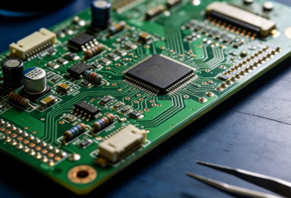
Design Verification and Manufacturing Preparation
4.1 Comprehensive Design Checklist
- Electrical Rule Check (ERC): Verify the correctness of electrical connections in the schematic
- Design Rule Check (DRC): Ensure compliance with manufacturing and assembly requirements
- Signal Integrity Analysis: Pre-check signal quality using simulation tools
- Power Integrity Analysis: Evaluate PDN performance
- Thermal Analysis: Predict circuit board thermal distribution
- Mechanical Assembly Check: Ensure compatibility with enclosures and connectors
4.2 Manufacturing File Preparation
- Gerber Files: Precise description of each circuit layer
- Drill Files: Information on through-hole and pad locations
- Assembly Drawings: Component location and orientation instructions
- Bill of Materials (BOM): Complete component list with specifications
- Test Specifications: Factory test requirements and procedures
Industry Trends and Future Outlook
5.1 Current PCB Design Trends
- High-Density Interconnect (HDI): Smaller apertures, finer trace width and spacing
- Flexible/Rigid-Flex Boards: New applications for bendable circuits
- Embedded Components: Embedding passive components within the board
- High-Frequency Material Applications: Special substrates for 5G and millimeter-wave circuits
5.2 Application of Artificial Intelligence in PCB Design
AI technology is transforming the PCB design process:
- Automatic Layout Optimization: Machine learning-based component placement
- Intelligent Routing Assistants: Predict and resolve routing conflicts
- Design Defect Prediction: Identify potential issues early
- Manufacturing Yield Optimization: Adjust design parameters based on factory data
5.3 Sustainable Development and Eco-Friendly Design
- Lead-Free Process Compatibility: Compliance with RoHS directives
- Material Recyclability: Selection of eco-friendly substrates and surface finishes
- Energy Efficiency Optimization: Reduce power consumption through design
- Long-Life Design: Enhance product reliability and reparability
Conclusion
PCB design is a comprehensive discipline that integrates electrical engineering, materials science, and manufacturing technology. With the rapid development of electronic technology, excellent designers need to continuously learn new tools, materials, and processes. Remember, every design challenge is an opportunity to improve skills, and every failure is a valuable process for accumulating experience.
Three Core Issues in PCB Design
A: Problem: High-speed signal deformation and crosstalk
Solutions:
1.Control impedance matching (calculate trace width and stack-up)
2.Place a complete ground plane adjacent to critical signals
3.Keep sensitive signal spacing ≥ 3 times the trace width
4.Prioritize short paths and minimize vias for high-speed signals
A: Problem: Unstable chip power supply, system abnormal reset
Solutions:
1.Use dedicated power/ground layers to reduce impedance
2.Place decoupling capacitors in “large-medium-small” order near chip power pins
3.Isolate digital and analog power with beads/0Ω resistors at a single point
A: Problem: EMC test failures, abnormal operation under high temperature
Solutions:
1.Minimize high-frequency signal loop area
2.Partition digital/analog/power ground and connect at a single point
3.Distribute heat-generating components and add thermal vias and copper pours