Designing a Printed Circuit Board (PCB) is a delicate balance between electrical engineering and physical manufacturing. In 2026, with the rise of high-speed signals and miniaturization, a “working” design is no longer enough—it must be an optimized design.
At HanSphere, we’ve analyzed thousands of design files. This guide shares our factory-floor insights to help you reduce revisions, lower costs, and ensure 100% reliability.
1. Fundamentals: Adhering to IPC Standards
Reliable PCBs start with industry-standard compliance. For most commercial and industrial applications, we recommend following:
Class 2 vs. Class 3: Most projects fall under Class 2, but for aerospace or medical, ensure your clearances meet Class 3 “High Reliability” specs.
IPC-2221: The foundation for all generic PCB design requirements.
IPC-6012: Qualification and performance specifications for rigid boards.
2. The Core Workflow: A Step-by-Step Approach
Step 1: Schematic Capture & ERC
Before the layout, ensure your netlist is flawless. Run an Electrical Rule Check (ERC) to catch floating pins or shorted nets early.
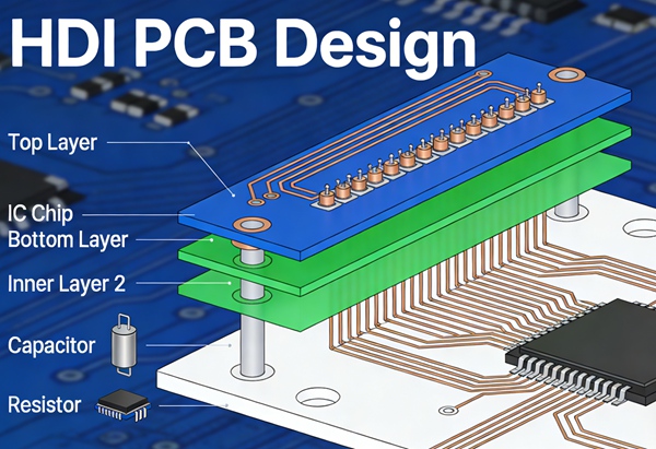
Step 2: PCB Stackup Design
The stackup is the “backbone” of your board.
- Pro Tip: For 4-layer boards, use a Signal-Ground-Power-Signal configuration to minimize EMI.
- Internal Link: Explore our PCB Manufacturing Capabilities to see our supported TG170 and specialized substrate options.
Step 3: Component Placement
Place high-speed components first, followed by connectors and power circuits. Keep decoupling capacitors as close to the IC power pins as possible.

3. Design for Manufacturing (DFM) Rules
To prevent production delays at the HanSphere factory, adhere to these critical tolerances:
| Feature | Standard Capability | High-Precision Capability |
| Min. Trace Width/Space | 3.5 / 3.5 mil | 2.0 / 2.0 mil |
| Min. Drill Size (Mechanical) | 0.2 mm | 0.15 mm |
| Min. Laser Drill (HDI) | 0.1 mm | 0.075 mm |
| Solder Mask Clearance | 2 mil | 1 mil |
4. Signal & Power Integrity (SI/PI)
In 2026, even simple boards often carry high-speed signals (USB-C, DDR4/5).
- Impedance Control: Use a 50Ω single-ended or 90/100Ω differential pair strategy.
- Thermal Vias: Don’t let your components overheat. Place thermal vias under power pads to sink heat into the internal ground planes.
5. How to Prepare Your Design for Production
- Run DRC (Design Rule Check):
Use HanSphere’s DRC settings in Altium or Allegro.
- Generate Gerber X2 or ODB++:
We prefer ODB++ as it contains more intelligent data, reducing CAM errors.
- Include a Readme File:
Specify your stackup, surface finish (ENIG, OSP, HASL), and copper weight (e.g., 1oz).
- Export Netlist:
This allows us to perform a “Comparison Test” against your Gerbers.
Frequently Asked Questions (FAQ)
A: Missing drill files or ambiguous layer stackups. Always provide a clear PDF or text file detailing your layer order.
A: Use ENIG (Electroless Nickel Immersion Gold) for fine-pitch SMT components and better shelf life. Use HASL (Hot Air Solder Leveling) for cost-sensitive, through-hole-heavy projects.
A: Yes. We offer end-to-end services. Check our PCB Assembly Guide for more details.
Conclusion
A great PCB design is the bridge between a brilliant idea and a reliable product. By following these DFM rules, you ensure your project moves seamlessly from the screen to the assembly line.
Get an Instant Quote at HanSphere