In modern electronics, Surface Mount Technology (SMT) is the gold standard for creating compact, high-performance devices. Whether you are building an IoT sensor or a complex server motherboard, the efficiency of your SMT assembly process determines your product’s reliability and cost.
At HanSphere, we operate high-speed, automated SMT lines designed for precision. In this guide, we walk you through the lifecycle of an SMT project and how to optimize your design for our machines.
1. What is SMT Assembly?
Unlike traditional Through-Hole Technology (THT), where components are inserted into drilled holes, SMT components are mounted directly onto the surface of the PCB. This allows for:
- Higher Component Density: Smaller devices and double-sided mounting.
- Improved Electrical Performance: Shorter lead lengths reduce parasitic capacitance and inductance.
- Lower Production Costs: Faster automation with fewer manual steps.
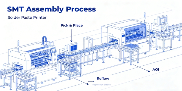
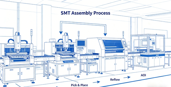
2. The 5-Step SMT Assembly Process at HanSphere
Step 1: Solder Paste Printing
The process begins with a stainless-steel stencil. We apply solder paste (a mix of flux and tiny solder balls) onto the PCB pads.
- Factory Detail: We use automated solder paste inspection (SPI) to ensure the volume and height of the paste are perfect before a single component is placed.
Step 2: High-Speed Pick and Place
Our automated machines use vacuum nozzles to pick components from reels and place them onto the solder paste with micron-level accuracy.
- 2026 Tech Update: Our lines now utilize AI-driven vision systems to detect component polarity and alignment in real-time, eliminating human error.
Step 3: Reflow Soldering
The boards enter a multi-zone reflow oven. The temperature is precisely controlled to melt the solder paste without damaging sensitive components, creating a solid mechanical and electrical bond.
Step 4: AOI & X-Ray Inspection
Quality is non-negotiable.
- AOI (Automated Optical Inspection): Scans for missing components, offsets, or solder bridges.
- AXI (Automated X-Ray Inspection): Essential for BGA (Ball Grid Array) components where the solder joints are hidden beneath the chip.
Step 5: Cleaning and Final Test
Depending on your requirements, we perform ultrasonic cleaning to remove flux residue and conduct Functional Circuit Testing (FCT) to ensure the board works exactly as intended.
3. Design for Assembly (DFA) Tips
To ensure a smooth run on our SMT lines, consider these factory-ready tips:
- Fiducial Marks: Place at least three fiducial marks on your PCB corners. Our machines use these “anchors” to calibrate their positioning.
- Panelization: If your board is smaller than 50mm, panelize it with “breakaway tabs” or “V-scores” to improve handling speed.
- Component Spacing: Leave enough “keep-out” zones around large components to allow the pick-and-place head and AOI cameras to see clearly.
4. SMT vs. THT: Which Should You Choose?
While SMT is dominant, Through-Hole Technology (THT) is still used for connectors, power transistors, and components that require strong mechanical bonds. HanSphere offers Hybrid Assembly, combining the speed of SMT with the durability of THT.
- Internal Link: See our Full PCBA Capabilities for a comparison chart.
FAQ: SMT Assembly Insights
A: For prototypes, we offer 24–72 hour “Quick-Turn” services. For mass production, lead times typically range from 2 to 4 weeks depending on component sourcing.
A: Yes. Our latest pick-and-place lines are fully capable of handling ultra-small passive components used in miniaturized wearables.
A: We offer three options: Full Turnkey (we source everything), Kitted (you provide everything), and Partial Turnkey (we source some, you provide some).