Rigid-flex PCBs offer the best of both worlds: the structural integrity of rigid boards and the spatial flexibility of flex circuits. However, they are also the most complex to manufacture.
At HanSphere, we see many designs fail due to “mechanical fatigue” or “trace cracking” at the transition zones. This guide focuses on the Design for Manufacturing (DFM) rules that ensure your rigid-flex project succeeds on the first pass.
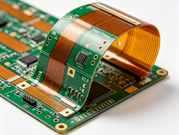
1. The Golden Rule: The Bend Radius
The most common failure in rigid-flex design is over-stressing the flexible substrate.
- Single-Sided Flex: Bend radius should be at least 6x the flex thickness.
- Double-Sided Flex: Bend radius should be at least 10x the flex thickness.
- Dynamic Flex (Repeatable Bending): Aim for 20x+ thickness to prevent copper work-hardening and eventual fracture.
2. Transition Zone Integrity
The area where the rigid board meets the flexible section is a high-stress point.
- Avoid Vias in the Transition: Never place vias or component pads within 50mil (1.27mm) of the rigid-to-flex interface.
- Strain Relief Fillets: Use rounded “fillets” at the transition points to distribute mechanical stress.
- Adhesive Coverage: Ensure the coverlay overlaps the rigid section by at least 30mil to prevent peeling.
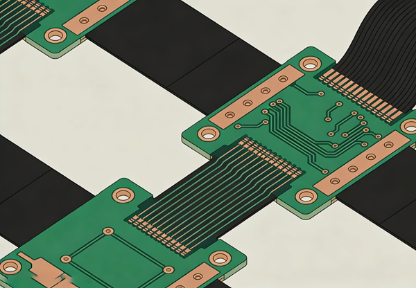
3. Advanced Routing Strategies
Flex circuits require a different routing philosophy than FR-4.
- Avoid 90-Degree Corners: Use rounded traces or 45-degree angles. Sharp corners act as “stress concentrators” where cracks begin.
- Staggered Traces: On double-sided flex, do not place traces directly on top of each other. Stagger them to reduce the “I-Beam” effect, which makes the board too stiff and prone to cracking.
- Hatched Ground Planes: Instead of solid copper pours, use a diamond hatch pattern for ground planes in the flex area. This maintains EMI shielding while preserving flexibility.
4. Optimized Rigid-Flex Stackup (Example)
A standard 4-layer rigid-flex stackup typically looks like this:
- Top Layer (Rigid): Signal / Components
- Internal Layer 2 (Flex): Ground / Signal (Polyimide Core)
- Internal Layer 3 (Flex): Power / Signal (Polyimide Core)
- Bottom Layer (Rigid): Signal / Components
HanSphere Factory Tip: We highly recommend using Adhesiveless Base Materials. They are thinner and more reliable for high-temperature lead-free soldering compared to traditional adhesive-based cores.
How to Prepare Your Files for HanSphere
- Define the Bend Requirements:
Mark the “Bend Lines” and “Bend Areas” clearly on a separate mechanical layer.
- Specify Coverlay Openings:
Use a 1:1 scale for coverlay openings to ensure precise solder mask alignment.
- Material Callouts:
Clearly define the Polyimide (PI) thickness and copper weight (e.g., 0.5oz is preferred for better flexibility).
- Final DRC:
Run a specific “Flex-Aware” DRC check if your software (like Altium) supports it.
Frequently Asked Questions (FAQ)
A: Yes, HanSphere uses high-quality FR-4 combined with Polyimide (Kapton) for the flexible layers to ensure thermal stability during assembly.
A: This is usually caused by a bend radius that is too tight or placing “termination points” (like vias) too close to the bend line.
A: Yes. We specialize in both rapid prototyping and mass production. Check our Rigid-Flex Capabilities for specific tolerance data.