Printed Circuit Boards (PCBs) are the backbone of almost every electronic device we use today, from smartphones and computers to medical devices and automobiles. But how exactly are these essential components designed? In this article, we’ll take you through the basics of PCB design, the design process, the tools you’ll need, and some industry insights. For companies looking to streamline the PCB design and manufacturing process, partnering with experienced service providers like Hansphere, a one-stop solution for PCB services, can offer valuable support throughout the entire journey.

What is PCB Design?
PCB design refers to the process of creating the layout and electrical connections of a printed circuit board. A PCB serves as a mechanical base for the components of an electronic system and connects them electrically through traces and pads. Whether it’s a simple LED circuit or a complex motherboard, every electronic device uses PCBs to ensure proper functionality.
A PCB is made up of a non-conductive material, often fiberglass, onto which a thin layer of conductive material, usually copper, is etched to form the electrical pathways. The process of designing these pathways, as well as placing and connecting components, is known as PCB design.
The PCB Design Process
The PCB design process can be broken down into several key stages:
1. Initial Design and Conceptualization
Before you even begin drawing your PCB, it’s crucial to define your design requirements. This includes deciding on the type of PCB you need (single-sided, double-sided, multi-layer), selecting components, and planning the overall layout. At this stage, you should also gather any necessary electrical specifications or system constraints.
Key steps in this phase include:
- Circuit Schematic Design: Creating a diagram of how the components are connected electrically.
- Component Selection: Choosing the right components (resistors, capacitors, ICs) for the design.
If you’re looking for a partner to help guide you through the early stages of PCB design, companies like Hansphere provide comprehensive services that assist with component sourcing, schematic review, and even concept prototyping to make the process smoother for you.
2. PCB Layout Design
The layout design is where the actual routing of the PCB takes place. It’s about deciding where each component will be placed on the board and how the electrical connections (traces) will be routed between them.
Key considerations include:
- Component Placement: Ensuring that components are placed efficiently and logically, with consideration for heat dissipation, signal integrity, and manufacturability.
- Routing: Drawing the electrical paths between components while maintaining a balance between signal integrity and design efficiency.
- Layer Stack-up: For multi-layer designs, the arrangement of the layers (signal layers, ground planes, power planes) must be optimized for performance.
During this phase, Hansphere can assist with the optimization of the PCB layout, offering professional feedback and utilizing their industry experience to ensure that your design meets both technical and production requirements.
3. Design Rule Checking (DRC) and Electrical Rule Checking (ERC)
Once the layout is done, it’s crucial to perform checks to ensure the design follows all the manufacturing and electrical rules. DRC ensures there are no design violations, such as traces that are too close together, while ERC checks for potential electrical problems, such as short circuits.
4. PCB Fabrication
After finalizing the design, the PCB goes into the fabrication process, where the physical board is manufactured. This involves:
- Etching Copper Layers: The unwanted copper is etched away, leaving behind the traces.
- Drilling Holes: Holes for component leads are drilled, often with laser precision.
- Lamination and Solder Masking: The PCB is coated with a solder mask, and component pads are added.
For businesses looking to ensure high-quality, efficient production, Hansphere offers end-to-end PCB manufacturing services, guaranteeing that your design is precisely fabricated and meets industry standards.
5. Assembly and Testing
The final step is the assembly phase, where components are soldered onto the PCB. After assembly, rigorous testing is conducted to ensure the board functions as intended. This includes electrical testing, as well as more detailed functional tests if the board is part of a larger system.
As part of its comprehensive PCB services, Hansphere also provides assembly and testing solutions, ensuring that your final product is fully functional and ready for deployment.
Common PCB Design Software and Tools
Designing PCBs requires the right tools, and fortunately, there are many powerful PCB design software packages available. Below are some of the most popular options:
1. Altium Designer
- Features: Altium Designer is one of the most advanced and feature-rich PCB design tools, offering a comprehensive suite for designing complex multi-layer PCBs. It supports 3D visualization, advanced routing, and extensive component libraries.
- Pros: Intuitive user interface, powerful design tools, great for complex designs.
- Cons: High learning curve and expensive for beginners.
2. Cadence Allegro
- Features: Cadence Allegro is a professional-grade PCB design tool, known for its high-level features in designing high-frequency and high-performance boards.
- Pros: Robust features, excellent for advanced routing, and signal integrity analysis.
- Cons: Complex interface, high cost.
3. KiCad
- Features: KiCad is an open-source PCB design tool that offers all the basic features needed to design PCBs. It is suitable for both beginners and more advanced users.
- Pros: Free to use, user-friendly, and highly customizable.
- Cons: Limited in comparison to paid software for more complex designs.
4. Autodesk Eagle
- Features: Autodesk Eagle is popular for hobbyists and smaller-scale PCB designs. It offers a simple interface and has been integrated with Fusion 360 for better 3D modeling.
- Pros: Easy to use, affordable for smaller projects.
- Cons: Lacks some advanced features compared to other professional tools.
Common Challenges in PCB Design
While PCB design might seem straightforward at first glance, it can quickly become complicated. Some of the most common challenges include:
1. Signal Integrity and Crosstalk
As designs become more complex, ensuring the integrity of high-speed signals can become a problem. To avoid issues like crosstalk or signal degradation, designers must carefully manage trace lengths, impedance, and ground planes.
2. Thermal Management
In high-power circuits, managing heat dissipation is crucial to prevent damage to components. Adequate placement of components and the use of heat sinks or thermal vias can help mitigate overheating issues.
3. Electromagnetic Interference (EMI)
EMI can interfere with the proper functioning of electronic systems. It’s essential to design PCBs with sufficient grounding and shielding to prevent unwanted electromagnetic interference.
4. Design for Manufacturability
A design that works perfectly in theory might not be easy or cheap to manufacture. It’s essential to work within the constraints of manufacturing processes, ensuring the PCB can be produced at a reasonable cost without sacrificing performance.
Hansphere, with its years of expertise in PCB design and manufacturing, can help mitigate many of these challenges by providing specialized advice, advanced design tools, and a deep understanding of the manufacturing process.
Applications of PCB Design in Different Industries
PCBs are ubiquitous and are found in almost every modern electronic device. Here are some key industries that rely heavily on PCB design:
1. Consumer Electronics
From smartphones to laptops, PCBs are at the heart of all consumer electronics. The challenge here is to design compact, efficient, and cost-effective boards that can handle a range of functions.
2. Automotive
With the rise of electric vehicles and advanced driver-assistance systems (ADAS), automotive PCBs are becoming increasingly sophisticated. These PCBs must be robust and capable of withstanding harsh conditions.
3. Medical Devices
Medical PCBs require high reliability and accuracy. Devices like pacemakers, diagnostic machines, and wearable health monitors all rely on PCB design to ensure proper functionality.
4. Industrial Applications
Industrial machines, robots, and automation systems rely on complex PCBs that control everything from power distribution to data communication.
Advanced PCB Design Trends
1. HDI (High-Density Interconnect) PCB
HDI boards are designed with smaller features and higher component density. This trend is driven by the need for smaller, more powerful devices.
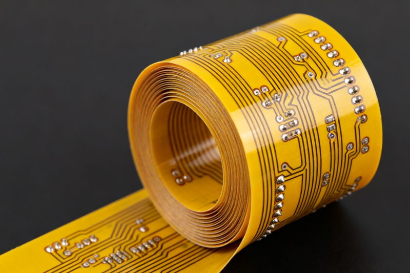
2. Flexible PCBs
Flexible PCBs allow for designs that can bend, twist, and fold. These are commonly used in wearable devices, medical implants, and foldable electronics.
3. PCB Design Automation
With advancements in AI and machine learning, PCB design automation is becoming a reality. These tools can automatically route traces, optimize component placement, and even identify potential issues in the design.
How to Become a Better PCB Designer
To become an expert PCB designer, continuous learning is essential. Here are some tips:
- Study Electronics Theory: A solid understanding of electronics will help you make better design decisions.
- Learn PCB Design Software: Practice using PCB design software and explore their advanced features.
- Experiment with Projects: Hands-on experience is invaluable. Start with small projects and gradually move to more complex designs.
- Stay Updated on Trends: PCB design is a constantly evolving field. Keeping up with the latest trends and technologies will help you stay competitive.
Conclusion
PCB design is both an art and a science, requiring a deep understanding of electronics, materials, and manufacturing processes. By following the right design process, using the appropriate tools, and staying updated on trends, you can create efficient and reliable PCBs for any application. Whether you’re designing a simple circuit or a complex system, mastering the PCB design process is crucial for building the electronic devices of the future. With the support of experts like Hansphere, who offer comprehensive PCB services from design to fabrication, your projects can move from concept to reality with ease.
Common FAQ (Frequently Asked Questions)
Starting PCB design can feel overwhelming if you’re new to the field, but breaking the process down into manageable steps can help:
Step 1: Understand Your Circuit
Before diving into design tools, ensure you have a solid understanding of the electronic circuit you’re designing. Create a schematic diagram that shows how all components are connected.
Step 2: Choose a PCB Design Tool
There are various PCB design software options available, such as Altium Designer, KiCad, or Autodesk Eagle. Choose one based on your project needs and experience level. For beginners, KiCad or Autodesk Eagle might be good options.
Step 3: Create a Schematic
Using your chosen tool, create a schematic that represents the electrical connections between components.
Step 4: Design the Layout
Once your schematic is ready, begin placing the components on the PCB layout. Consider factors like component placement, routing, and signal integrity.
Step 5: Run Design Rule Checks (DRC)
After the layout is complete, run DRC to ensure your design meets all manufacturing standards and electrical rules.
Step 6: Fabrication and Assembly
Finally, send your design files to a PCB manufacturer. Many services, like Hansphere, offer both fabrication and assembly, ensuring a seamless process from design to production.
A multilayer PCB is a type of PCB that contains more than two layers of conductive material (often copper) and insulating layers. These boards are used for complex circuits that require higher component density, such as smartphones, computers, and medical devices.
Key features of multilayer PCBs:
Stacked Layers: Multilayer PCBs consist of three or more conductive layers separated by insulating material (often fiberglass).
High Density: Multilayer PCBs allow for more compact and high-density designs. This is particularly important for devices where space is limited but complexity is high.
Improved Performance: Multilayer boards help reduce electromagnetic interference (EMI) and provide better signal integrity for high-speed circuits.
Multilayer PCBs are more expensive to produce due to the complexity of manufacturing, but they are essential for advanced electronics.
There are several common mistakes PCB designers make, but they can be easily avoided with careful planning and attention to detail:
1. Improper Component Placement:
Avoid placing components too close together or in areas where heat dissipation is poor. Ensure there’s enough space for proper routing and manufacturing processes.
2. Not Considering Signal Integrity:
Pay attention to the routing of high-speed signals. Improper trace width, grounding, and impedance mismatches can result in signal loss or distortion.
3. Neglecting Power and Ground Planes:
Power and ground planes are essential for stable and noise-free operation. Make sure to properly design these planes, especially in high-frequency or high-power circuits.
4. Ignoring Design Rules and DRC Checks:
Always run design rule checks (DRC) to ensure that your design meets the manufacturing standards. Many design issues, such as trace width violations or unconnected nets, can be caught early through DRC.
5. Overlooking Thermal Management:
If your circuit generates a lot of heat, be sure to design for thermal dissipation. This includes using heat sinks, thermal vias, and appropriate component placement to prevent overheating.
6. Not Considering Manufacturing Constraints:
Always design with the manufacturing process in mind. For example, check the minimum trace width, hole sizes, and the number of layers that your PCB manufacturer can handle.
By being mindful of these factors and working with experienced partners, such as Hansphere, you can avoid many of the common pitfalls and create reliable and efficient PCBs.