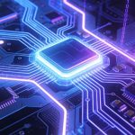
The printed circuit board (PCB) is one of the most underrated technological marvels of the 21st century. While the world generates 2.5 trillion bytes of data daily, PCBs serve as the physical channels for this data flow, carrying critical functions from smartphones to supercomputers, and from medical devices to spacecraft. They are not merely platforms for connecting electronic components but comprehensive solutions integrating signal, power, and thermal management.
What is a PCB?
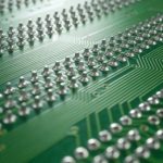
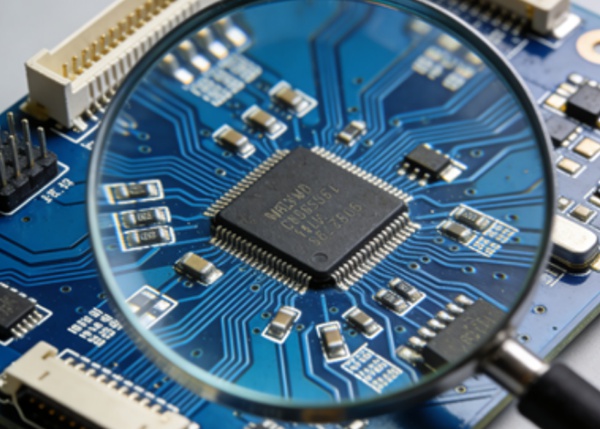
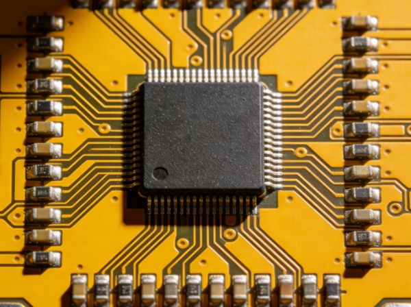
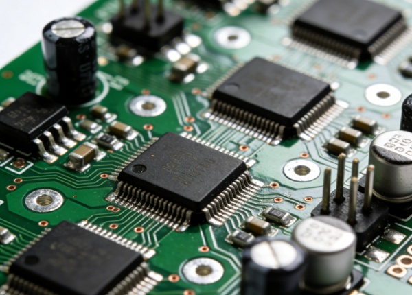
A printed circuit board (PCB) is a substrate used for both mechanical support and electrical interconnection of electronic components. By replacing traditional hand-wiring with pre-designed copper trace networks, it enables the miniaturization, high reliability, and mass production of electronic products.
The Technical Architecture of PCBs
1. Substrate Revolution: From FR-4 to High-Frequency Specialty Materials
Modern PCB materials science has moved beyond traditional glass fiber epoxy resin (FR-4). In 5G millimeter-wave applications, Rogers RO3003 material provides a stable dielectric constant (εᵣ=3.0±0.04), reducing 28GHz signal loss to 0.0013dB/mm. Flexible polyimide substrates enable foldable phones with a bending lifespan exceeding 200,000 cycles.
2. Conductive Layer Evolution: Ultra-Fine Line Technology
High-end server PCBs have entered the 15-micron line width era (equivalent to the diameter of a red blood cell). Intel’s Eagle Stream platform employs a 20-layer PCB with over 8,000 vias, achieving a PCIe 5.0 signal transmission rate of 32GT/s and impedance control accuracy of ±5%.
3. Three-Dimensional Stacking: From 2D to 3D
In Apple’s M2 Ultra chip packaging, the hybrid use of silicon interposers and PCBs creates a new interconnect paradigm:
- Line density: 1,300 signal lines/cm²
- Interlayer alignment accuracy: ±8 microns
- Coefficient of thermal expansion matching: CTE difference <3ppm/°C
Engineering Solutions for Five Core Challenges
Challenge 1: The Spatio-Temporal Game of Signal Integrity
In 56Gbps PAM4 signal systems, the timing budget is only 18ps. Solutions include:
- Differential pair length matching: ±2mil tolerance
- Back-drilling technology: Eliminating via stubs (Stub<8mil)
- Loss compensation: Pre-emphasis + equalizer joint optimization
Challenge 2: Multi-Dimensional Optimization of Power Integrity
AMD EPYC processors have transient currents up to 200A with voltage tolerance of ±3%. Key technological breakthroughs:
- Full copper-clad power layers: DC impedance <0.5mΩ
- Distributed decoupling network: 100nF+10nF+1nF capacitor matrix
- Bead isolation: Digital and analog power isolation >60dB
Challenge 3: Phase-Change Intelligence in Thermal Management
GPU power density has reached 2W/mm², with innovative solutions:
- Embedded heat pipes: Thermal conductivity increased to 5000W/mK
- Phase change materials: Latent heat absorption for instantaneous thermal shocks
- 3D printed heat sinks: Customized microchannel designs
Challenge 4: Systems Engineering for Electromagnetic Compatibility
Emission control in automotive radar PCBs:
- Split ground planes: Single-point connection for digital and RF grounds
- Shield cavity design: Isolation >80dB @77GHz
- Edge plating: Reducing edge radiation
Challenge 5: The Physical Limits of Reliability
Aerospace-grade PCB design standards:
- Thermal cycle testing: -55°C to 125°C, 1000 cycles
- Vibration rating: 20G RMS, three axes
- Void rate control: Solder voids <10%
Digital Transformation of the Design Process
AI-Driven Design Revolution
Cadence Cerebrus system achievements:
- Layout optimization time: Reduced from 2 weeks to 8 hours
- Routing success rate improvement: 37%
- Signal integrity violations reduction: 29%
Cloud Collaborative Design Platform
Altium 365 platform features:
- Real-time design rule checking
- Intelligent supply chain matching
- Version control and team collaboration
Frontier Breakthroughs in Manufacturing Technology
1. mSAP Process (Modified Semi-Additive Process)
For 5G millimeter-wave antenna arrays:
- Minimum line width: 8 microns
- Surface roughness: Rz<1 micron
- Yield improvement: 15%
2. Embedded Component Technology
Burying 0603 package resistors and capacitors within the board:
- Space saving: 30%
- Inductance reduction: 40%
- Reliability improvement: Resistant to mechanical stress
3. Heterogeneous Integration
TSMC’s 3DFabric technology:
- Silicon interposer: 4x redistribution layer density
- Hybrid bonding: Pitch <10 microns
- Thermal through vias: Thermal conductivity improved 3x
Sustainable Development: The Technological Path for Green PCBs
Eco-Friendly Material Innovations
- Halogen-free substrates: Compliant with IEC 61249-2-21 standard
- Bio-based resins: Carbon footprint reduced by 40%
- Recyclable metals: Copper recovery rate >95%
Energy-Saving Manufacturing Processes
- Direct imaging: Energy consumption reduced by 30%
- Cyanide-free gold plating: Zero toxic emissions
- Water circulation systems: Water savings of 65%
Industry Applications and Market Insights
Data Centers: High-Performance Computing PCB Market Annual Growth of 21%
- 112G SerDes channels: Loss <0.8dB/inch @28GHz
- Power modules: Efficiency >95%
- Thermal interface materials: Thermal resistance <0.1°C·cm²/W
New Energy Vehicles: Automotive PCB Compound Growth Rate of 18%
- Battery management systems: 16-layer thick copper PCB (6oz)
- Autonomous driving: Radar PCB dielectric constant ±1% tolerance
- 800V fast charging: Creepage distance >3.2mm
Future Trends: 2025-2030 Technology Roadmap
Quantum Computing Interfaces
- Superconducting PCBs: Operating temperature 4K
- Microwave resonators: Q factor >10⁶
- Magnetic flux vortex control: Isolation >100dB
Neuromorphic Computing
- Brain-like interconnects: Three-dimensional mesh structures
- Memristor integration: Memory and computing integration
- Event-driven circuits: Energy consumption reduced 1000x
Self-Healing Systems
- Microcapsule technology: Automatic crack repair
- Shape-memory polymers: Deformation recovery rate >95%
- Electrochemical deposition: Open circuit self-repair
Professional Resources and Learning Pathways
Certification Systems
- IPC CID/CID+: Design certification
- IPC CIS: Soldering expert certification
- IEEE EMC certification: Electromagnetic compatibility expert
Simulation Tool Stack
- Signal integrity: ANSYS HFSS, Cadence Sigrity
- Thermal analysis: FloTHERM, Icepak
- Structural analysis: Abaqus, ANSYS Mechanical
Industry Standard Evolution
- IPC-2581: Intelligent data exchange format
- IPC-2152: New current-carrying capacity standard
- IEC 61189-3: High-frequency test methods
Conclusion
In the era of artificial intelligence, the Internet of Things, and quantum computing, PCBs are evolving from passive connection platforms to active performance engines. They are not just the infrastructure of circuits but also:
- Precise guides for electromagnetic energy
- System optimizers for heat dissipation
- Physical guarantors of reliability
- Spatial carriers of innovation
For electronic engineers, mastering PCB design is not only a technical capability but a core literacy connecting physical laws with engineering innovation. Each PCB optimization redefines the relationship between information, energy, and space—making this one of the most profound and creative fields in electronic engineering.
PCB Frequently Asked Questions
A: Symptoms: High-speed signal deformation, timing errors
Solutions: Impedance control, shorten traces, place ground planes near critical signals, follow 3W spacing rule
A: Symptoms: Unstable chip power supply, system anomalies
Solutions: Dedicated power layers, hierarchical decoupling capacitors (large/medium/small combinations), isolate digital/analog power
A: Symptoms: EMC test failures, high-temperature anomalies
Solutions: Minimize signal loops, partition ground planes, distribute heat-generating components, add thermal vias