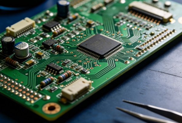
Printed Circuit Boards (PCBs) are the silent pulse of modern innovation. From the high-frequency demands of 5G infrastructure to the compact constraints of wearable medical devices, a well-designed PCB is the difference between a high-performing product and a costly prototype failure.
In this guide, we’ll move beyond the basics. Drawing from over a decade of hands-on experience at Hansphere, we will explore the professional PCB design lifecycle, the tools used by industry veterans, and the critical “Design for Manufacturing” (DFM) principles that ensure your project moves seamlessly from screen to silicon.

1. Defining PCB Design: More Than Just Traces
At its core, PCB design is the art of translating a theoretical circuit into a physical, manufacturable reality. It involves placing components on a non-conductive substrate and “routing” electrical connections using copper tracks.
However, modern design isn’t just about connectivity; it’s about Signal Integrity (SI) and Power Integrity (PI). A professional designer must account for parasitic capacitance, impedance mismatch, and thermal bottlenecks before a single board is ever etched.
2. The Professional Design Lifecycle
Phase 1: Schematic Capture & Logic
The schematic is your roadmap. It defines the logical connections between components.
- Pro Tip: Always perform a Footprint Check at this stage. There is nothing worse than finishing a complex layout only to realize your IC footprint doesn’t match the physical part.
- Related: For high-complexity projects, ensure your PCB Design partner reviews the netlist for logical errors early on.
Phase 2: Layer Stack-up & Layout Strategy
For boards beyond two layers, the “Stack-up” is critical. You must decide where the signal, ground, and power planes sit.
- Expert Insight: Using a solid ground plane directly adjacent to high-speed signal layers is the most effective way to reduce Electromagnetic Interference (EMI).
- Explore: Learn more about high-density routing in our HDI-PCB specialized guide.
Phase 3: Routing and Signal Integrity
Routing is where the “art” happens. Designers must balance trace widths for current-carrying capacity against the space constraints of the board.
- Critical Factor: In High Frequency PCBs, controlled impedance is mandatory to prevent signal reflection.
Phase 4: Design for Manufacturing (DFM)
This is the “Hansphere Standard.” A design might work in a simulator, but can it be built? DFM checks ensure that drill hits aren’t too close to copper traces and that the solder mask doesn’t interfere with pad connectivity.
3. Essential Tools of the Trade
Choosing the right software depends on your project’s complexity:
- Altium Designer: The industry standard for professional-grade, multi-layer, and high-speed designs.
- KiCad: A powerful, open-source alternative that is rapidly gaining traction in the engineering community.
- Cadence Allegro: Favored by enterprise-level teams for advanced signal analysis.
- Comparison: Check out our full breakdown of PCB Design Tools.

How to Design a Manufacturable PCB in 5 Steps
Target: Beginners to Intermediate Engineers
Total Time: Variable (Project dependent)
- Step 1: Finalize the Schematic and BOM
Ensure all components are sourced and available. Use a Bill of Materials (BOM) management tool to avoid “End of Life” (EOL) components.
- Step 2: Define Board Constraints
Set your board outline, mounting hole positions, and keep-out zones. Consult your PCB Manufacturing partner for their minimum trace width and spacing capabilities.
- Step 3: Strategic Component Placement
Place critical components first—connectors, high-speed processors, and power regulators. Keep noisy components (like switching regulators) away from sensitive analog signals.
- Step 4: Route the Connections
Route high-speed signals first, followed by general-purpose I/O. Finally, pour your ground and power planes to provide a stable reference.
- Step 5: Generate Gerber Files and DFM Check
Export your design as Gerber RS-274X or ODB++ files. Run a final Design Rule Check (DRC) to catch any lingering clearance issues before submission.
Overcoming Common Challenges
- Thermal Management: For power-heavy boards, use thermal vias to move heat from the top layer to internal copper planes. If using flexible substrates, see our Flex-PCB design tips.
- Crosstalk: Maintain a distance of at least 3x the trace width between parallel high-speed lines to minimize inductive coupling.
- Cost Optimization: Reducing the layer count or avoiding ultra-small vias can significantly lower PCB Assembly costs.
5. Industry Trends: What’s Next?
The industry is moving toward Rigid-Flex designs for foldables and Ceramic PCBs for extreme temperature environments. Additionally, AI-assisted routing is starting to shorten the design cycle for non-critical signal paths.
Learn more: Rigid-Flex PCB Benefits | Ceramic PCB Applications.
Frequently Asked Questions (FAQ)
A: Ignoring the return path. Every signal has a return current; if you don’t provide a clear path (ideally a ground plane), the signal will find its own way, creating EMI and noise.
A: Simple designs work on 1-2 layers. Complex digital designs with high-speed buses (like DDR4 or PCIe) typically require 4 to 12 layers to maintain signal integrity and power distribution.
A: While 3D printing is excellent for CNC Services and enclosures, it is currently mostly used for prototyping conductive traces rather than mass-producing high-density boards.
Conclusion
PCB design is a balancing act between electrical performance, mechanical constraints, and manufacturing costs. By prioritizing DFM and understanding the physics of your signals, you can reduce revision cycles and get your product to market faster.
Ready to turn your design into reality? At Hansphere, we provide end-to-end support—from initial design consultation to final assembly. Contact us today for a professional design review.