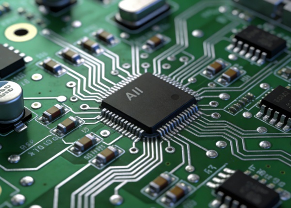
Artificial intelligence is increasingly influencing electronic design automation, but its role in PCB design is often misunderstood. Rather than replacing engineers or fully automating design processes, AI is emerging as a supportive technology—enhancing efficiency, consistency, and early decision-making in complex PCB projects.
This pillar page provides a structured overview of AI PCB design, explaining how machine learning is applied across layout, routing, signal integrity, power integrity, and design workflows. Each section links to in-depth technical articles that explore specific applications and limitations.

What Is AI PCB Design?
AI PCB design refers to the use of machine learning and data-driven algorithms to assist engineers during the PCB design process. These systems analyze historical design data, layout patterns, and constraint relationships to support—not replace—traditional EDA tools.
Key characteristics of AI-assisted PCB design include:
- Pattern recognition from prior designs
- Early-stage risk detection
- Automated suggestions under defined constraints
- Continuous improvement through feedback data
AI does not eliminate physics-based simulation or engineering judgment. Instead, it enhances productivity by reducing repetitive tasks and highlighting potential issues earlier.
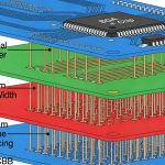
How AI Improves PCB Layout and Routing
PCB layout and routing are among the most time-consuming stages of board design, particularly for high-speed and high-density applications. AI-assisted tools help by analyzing connectivity, signal priority, and spatial constraints to generate optimized placement and routing suggestions.
Common benefits include:
- Shorter critical signal paths
- Reduced routing congestion
- More consistent design quality across projects
However, engineers must still validate AI-generated results before final sign-off.
🔗 Deep dive:
How AI Improves PCB Layout and Routing for High-Speed and High-Density Boards
AI Applications in Signal Integrity and Power Integrity
Signal integrity (SI) and power integrity (PI) are critical challenges in modern PCB design. AI supports SI and PI analysis by identifying risk patterns early—before full simulation—allowing engineers to prioritize the most critical nets and power structures.
Typical applications include:
- Predicting impedance discontinuities
- Highlighting crosstalk-prone regions
- Screening PDN weaknesses
AI enhances efficiency but does not replace physics-based simulation or validation.
🔗 Technical analysis:
Machine Learning Applications in PCB Signal Integrity and Power Integrity Analysis
AI Tools for PCB Design Engineers
Most AI functionality is delivered through features embedded within existing EDA platforms rather than standalone systems. These AI tools assist engineers in layout, routing, rule optimization, and early analysis.
AI tools are particularly effective for:
- High-speed digital designs
- Multi-layer, high-density boards
- Teams seeking workflow consistency
Understanding the capabilities and limitations of these tools is essential for successful adoption.
🔗 Tool-focused overview:
AI Tools for PCB Design Engineers: Features, Limitations, and Use Cases
The Future of AI in PCB Design Automation
The future of AI in PCB design will be shaped by deeper integration with EDA platforms and tighter links between design and manufacturing data. Rather than disruptive change, progress will remain incremental and engineer-driven.
Key future trends include:
- AI-assisted design constraint optimization
- Early risk prediction during layout
- Manufacturing feedback loops improving design decisions
Human expertise will remain central, with AI acting as an intelligent assistant.
🔗 Forward-looking perspective:
The Future of AI in PCB Design Automation and Electronic Manufacturing
How Engineers Should Approach AI PCB Design
To benefit from AI-assisted PCB design, engineers and organizations should:
- Treat AI as a decision-support tool, not an authority
- Maintain strong fundamentals in SI, PI, and manufacturing
- Validate all AI-generated recommendations
- Invest in workflow integration and training
AI adoption is most successful when aligned with engineering best practices rather than positioned as a replacement.
Conclusion
AI PCB design represents an evolution of electronic design automation, offering meaningful efficiency gains and early insight into complex design challenges. When used responsibly, AI enhances—not replaces—the role of PCB design engineers.
This pillar page serves as a central reference for understanding how AI is applied across modern PCB design workflows, with detailed articles exploring each area in depth.