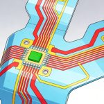
As electronic systems continue to increase in complexity, traditional PCB layout and routing workflows are approaching their practical limits. High-speed interfaces, increased component density, and multi-layer stackups place growing pressure on signal integrity, EMI control, and design efficiency.
AI PCB layout and routing technologies are emerging as effective engineering tools rather than experimental concepts. By applying machine learning algorithms to placement optimization and routing decision-making, engineers can reduce design iterations, improve consistency, and better manage high-speed and high-density PCB challenges.
This article explains how AI improves PCB layout and routing, focusing on real-world engineering benefits for modern electronic designs.
🔗 This article is part of the broader topic:
[AI PCB Design: Practical Applications of Machine Learning in Modern Electronics]

Why Traditional PCB Layout and Routing Are No Longer Enough
Conventional PCB layout and routing rely heavily on manual decisions and fixed design rules. While experienced engineers can achieve excellent results, modern designs introduce challenges such as:
- High-speed interfaces (USB4, PCIe Gen5, DDR5)
- Tight impedance control and length matching
- Limited routing space in high-density layouts
- Increased risk of crosstalk and EMI
As board complexity increases, manual routing often leads to repeated design–simulation–revision cycles. Signal integrity and power integrity issues are frequently discovered late in the process, increasing development time and cost.
This is where AI-driven PCB design automation provides measurable improvements.
AI-Driven PCB Layout Optimization
Intelligent Component Placement Using AI
Component placement has a direct impact on routing complexity, signal integrity, and thermal performance. AI-based placement tools use machine learning models trained on historical PCB designs to evaluate relationships between components, signal paths, and performance constraints.
AI-assisted placement can:
- Minimize critical signal path lengths
- Reduce unnecessary vias and layer transitions
- Improve grouping of functional blocks
- Enhance manufacturability and thermal balance
In high-speed PCB design, these early placement decisions significantly reduce downstream routing conflicts and SI risks.
Constraint-Aware Layout Decisions
Unlike traditional auto-placement features, AI-driven systems can evaluate multiple constraints simultaneously, including:
- Signal integrity and impedance requirements
- Power distribution efficiency
- EMI and noise coupling risks
- Manufacturing design rules
This multi-objective optimization is especially valuable in high-density PCB layouts, where trade-offs between routing space and electrical performance are unavoidable.
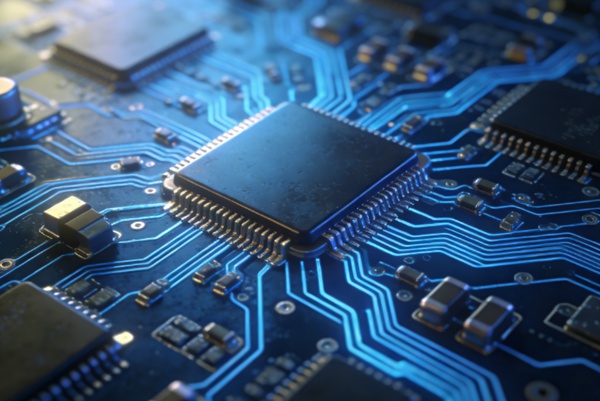
AI-Driven PCB Routing for High-Speed Signals
Automated Routing with Signal Integrity Awareness
AI-driven PCB routing goes beyond simple path optimization. Machine learning models can predict potential signal integrity problems based on routing patterns observed in previous designs.
Key routing improvements include:
- Intelligent differential pair routing
- Automated length matching for high-speed buses
- Early detection of impedance discontinuities
- Routing path recommendations based on SI risk
These capabilities allow engineers to address common high-speed PCB routing challenges earlier in the design cycle.
🔗 For a deeper technical discussion, see:
Machine Learning Applications in PCB Signal Integrity and Power Integrity Analysis
Reducing Crosstalk and EMI Risks
In dense PCB designs, crosstalk and electromagnetic interference are common failure points. AI-based routing systems analyze trace spacing, reference planes, and return paths to predict noise coupling risks.
When potential EMI issues are detected, AI tools can recommend alternative routing layers, spacing adjustments, or reference plane changes—helping engineers avoid costly redesigns during compliance testing.
Practical Benefits of AI PCB Layout and Routing
From real-world engineering projects, AI-assisted PCB layout and routing offer several practical advantages:
- Fewer design iterations through early issue detection
- Improved signal integrity for high-speed interfaces
- Shorter development cycles via automation
- More consistent design quality across teams
These benefits are particularly relevant for multi-layer boards used in data communication, industrial electronics, and consumer devices.
Limitations and the Role of Engineering Judgment
Despite its advantages, AI-driven PCB layout and routing do not replace engineering expertise.
Key limitations include:
- Dependence on high-quality training data
- Reduced effectiveness for unconventional designs
- Need for manual validation and final verification
AI should be treated as a design assistant, not an autonomous decision-maker. Experienced engineers remain responsible for validating routing strategies, stackups, and system-level performance.
🔗 For an overview of available solutions, see:
AI Tools for PCB Design Engineers: Features, Limitations, and Use Cases
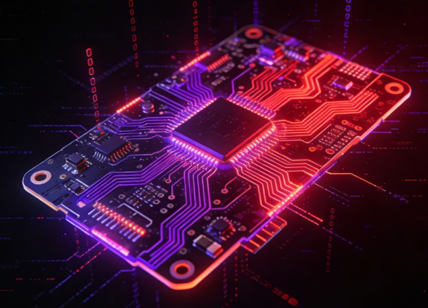
How This Fits into the Future of PCB Design
AI-assisted layout and routing represent an important step toward intelligent electronic design automation. As AI tools mature, placement, routing, simulation, and rule optimization will become increasingly integrated.
Understanding AI PCB layout and routing techniques is becoming essential for engineers working on high-speed and high-density designs.
🔗 Related perspective:
The Future of AI in PCB Design Automation and Electronic Manufacturing
Conclusion
AI improves PCB layout and routing by addressing the core challenges of modern electronics: complexity, speed, and density. Through intelligent component placement, signal-aware routing, and predictive analysis, AI-driven PCB design enables more reliable boards with shorter development cycles.
As a key entry point in the AI PCB design content cluster, this article establishes the practical foundation for understanding how machine learning is reshaping PCB layout and routing workflows.
FAQ – AI PCB Layout and Routing
A: No. AI-driven PCB layout and routing tools are designed to assist, not replace, experienced engineers. While AI can automate placement, routing suggestions, and early signal integrity analysis, final validation, stackup decisions, and compliance checks still require engineering judgment.
AI is most effective when used as a design assistant that accelerates workflows and reduces repetitive tasks.
A: AI improves high-speed PCB layout by analyzing historical design patterns and applying machine learning to optimize component placement and signal paths. This helps reduce critical trace lengths, minimize vias, and improve impedance consistency—key factors for maintaining signal integrity in interfaces such as PCIe, USB4, and DDR memory.
A: AI-driven PCB routing can be highly effective for complex multi-layer boards, especially when combined with well-defined design constraints. Machine learning models can predict routing conflicts, crosstalk risks, and impedance discontinuities early in the design process.
However, engineers must still review routing results and perform simulation-based verification for high-speed and high-density designs.
A: AI-assisted PCB layout and routing provide the greatest benefits for:
High-speed digital PCBs
High-density multi-layer boards
Designs with strict signal integrity requirements
Projects with tight development timelines
For simple or low-speed boards, traditional manual workflows may already be sufficient.
A: Yes, AI can help reduce EMI and crosstalk by analyzing trace spacing, routing layers, and reference planes. AI-based routing tools can identify potential noise coupling risks and suggest alternative routing strategies before physical prototyping.
That said, final EMI compliance still depends on careful validation and testing.
A: AI PCB design tools can be beneficial for both large and small teams. For smaller teams, AI-assisted automation helps reduce design time and reliance on manual iteration. However, tool cost, learning curve, and integration with existing workflows should be evaluated carefully.
A: AI-assisted layout and routing are foundational elements of next-generation electronic design automation. Future workflows are expected to integrate AI-driven placement, routing, simulation, and rule optimization into unified design environments, enabling faster and more reliable PCB development.