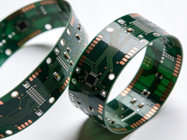
Flexible PCB failures are often intermittent, difficult to reproduce, and expensive to diagnose. Unlike rigid boards, flex circuits fail primarily due to mechanical stress, material fatigue, and manufacturing interactions rather than simple electrical overload.
This article focuses on flexible PCB failure analysis and root cause investigation, providing engineers with a structured approach to identifying failure mechanisms and preventing recurrence.
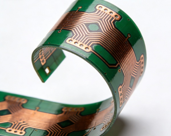
🔗 Part of the Flexible PCB Design Series
Flexible PCB Design: Materials, Layout, Reliability, and Manufacturing
Why Flexible PCB Failures Are Hard to Diagnose
Flex PCB failures commonly:
- Appear after extended use
- Pass initial electrical tests
- Occur only under mechanical stress
These characteristics make traditional troubleshooting ineffective.
Common Failure Modes in Flexible PCBs
Copper Trace Cracking
Symptoms
- Intermittent opens
- Resistance fluctuation
Root Causes
- Bend radius too small
- Traces routed parallel to bend lines
- ED copper in dynamic flex zones
🔗 Related design cause:
Bend Radius and Mechanical Reliability in Flexible PCB Design
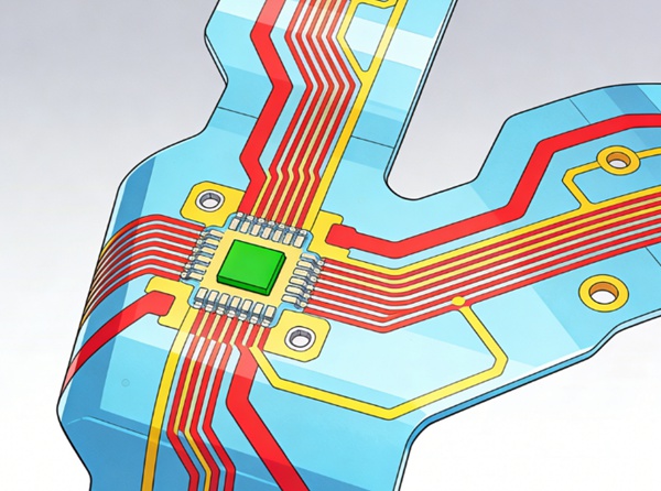
Via and Interconnect Failures
Symptoms
- Complete opens after assembly
- Failures after thermal cycling
Root Causes
- Vias placed in flex areas
- Poor plating adhesion
- Excessive mechanical stress
Delamination and Layer Separation
Symptoms
- Visual bubbling
- Loss of insulation resistance
Root Causes
- Adhesive flow issues
- Incompatible materials
- Excessive lamination stress
Coverlay Cracking and Lift
Symptoms
- Exposed copper
- Localized corrosion
Root Causes
- Coverlay openings near bend zones
- Poor adhesive bonding
- Excessive flexing
Structured Failure Analysis Methodology
Step 1: Failure Reproduction
- Identify operating conditions
- Recreate bending, thermal, and environmental stress
- Log cycle counts and angles
Step 2: Non-Destructive Inspection
- Optical inspection
- X-ray analysis
- Electrical continuity under bending
Step 3: Cross-Section Analysis
- Examine copper cracks
- Identify delamination zones
- Inspect via barrel integrity
Cross-sectioning often reveals failures invisible externally.
Step 4: Root Cause Mapping
Correlate failures with:
- Bend location
- Stackup structure
- Layout features
- Manufacturing processes
Linking Failures Back to Design Decisions
Most failures trace back to early design choices:
- Inadequate material selection
- Improper stackup symmetry
- Poor layout in bend areas
- Manufacturing constraints ignored
🔗 Design foundation:
Flexible PCB Materials and Stackup Design
Flexible PCB Layout Guidelines and Best Practices
Preventive Design Strategies
To prevent repeat failures:
- Redesign bend zones conservatively
- Use RA copper in dynamic flex areas
- Move vias and pads out of flex regions
- Validate with realistic mechanical testing
Documentation and Knowledge Retention
Failure analysis is only valuable if documented.
Best practices:
- Record failure mode images
- Link root causes to design rules
- Update internal design checklists
This transforms failures into institutional knowledge.
Conclusion
Flexible PCB failure analysis requires a multidisciplinary approach combining mechanical understanding, materials science, and manufacturing insight. By applying structured root cause investigation, engineers can not only fix failures but systematically prevent them in future designs.
This article completes the Flexible PCB Design expertise cluster.
FAQ – Flexible PCB Failure Analysis
A: Mechanical fatigue accumulates over time and is not detected by static testing.
A: Copper trace cracking in bend areas.
A: Yes. Most flex PCB failures originate from early design decisions.
A: No. Many failures require cross-section or stress testing to identify.
A: By bending the PCB under controlled conditions while monitoring continuity.
A: Immediately after detecting field or pilot production failures.