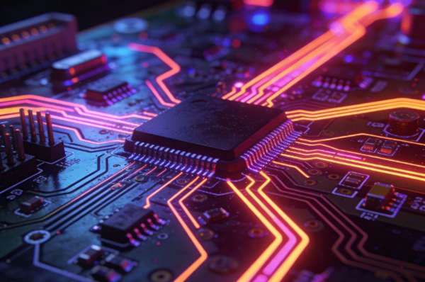
Artificial intelligence is gradually reshaping electronic design automation, but its impact on PCB design is often misunderstood. Rather than replacing engineers, AI is evolving as a supportive layer—enhancing decision-making, improving efficiency, and reducing repetitive tasks.
This article explores the future of AI in PCB design automation and electronic manufacturing, focusing on realistic developments, technical constraints, and how engineers should prepare for AI-assisted workflows.
🔗 This article concludes the core topic:
AI PCB Design: Practical Applications of Machine Learning in Modern Electronics
AI as an Evolution of EDA, Not a Replacement
The future of AI in PCB design lies in incremental integration, not disruption. Traditional EDA tools remain grounded in physics-based models, rule engines, and simulation. AI complements these foundations by learning from data rather than replacing established principles.
In practice, AI will increasingly act as:
- A recommendation engine for layout and routing decisions
- A risk-filtering layer before simulation
- A consistency enforcer across large design teams
Engineers will remain responsible for final validation and trade-off decisions.
Emerging Trends in AI-Assisted PCB Design
Deeper Integration into EDA Platforms
AI capabilities are expected to become native features within mainstream EDA tools rather than standalone add-ons. Placement, routing, and early analysis may share a unified AI-assisted interface, reducing context switching.
🔗 Related foundation:
AI Tools for PCB Design Engineers: Features, Limitations, and Use Cases
AI-Guided Design Constraint Optimization
Future AI systems may dynamically adjust design rules based on layout context. Instead of static constraints, AI could suggest optimized spacing, impedance targets, or via strategies based on prior successful designs.
This approach could reduce over-constraining and improve design efficiency.
Early Design Risk Prediction
AI will increasingly focus on early-stage risk identification. By analyzing partial layouts, AI models may flag potential SI, PI, or EMI concerns before full simulation is required.
🔗 Technical background:
Machine Learning Applications in PCB Signal Integrity and Power Integrity Analysis
AI and the PCB Manufacturing Feedback Loop
One of the most promising future developments is tighter integration between PCB design and manufacturing data.
AI systems could analyze fabrication yield, assembly defects, and field performance to inform future design recommendations. This feedback loop may help engineers:
- Improve manufacturability
- Reduce iteration cycles
- Align design choices with real-world outcomes
Such integration depends heavily on data availability and standardization.
Challenges and Constraints for AI Adoption
Data Quality and Accessibility
AI performance depends on large, high-quality datasets. In PCB design, data is often fragmented across companies, tools, and formats. Without standardized data pipelines, AI adoption will remain uneven.
Trust, Transparency, and Explainability
Engineers must understand why AI suggests a particular solution. Black-box recommendations without explainable logic are unlikely to gain widespread acceptance in safety- or reliability-critical designs.
Skill Evolution for PCB Engineers
As AI tools mature, PCB engineers will need to develop new skills, including:
- Interpreting AI recommendations
- Defining effective constraints for AI-assisted workflows
- Balancing automation with manual expertise
AI literacy will become part of professional competency—not a replacement for engineering fundamentals.
🔗 Workflow perspective:
How AI Improves PCB Layout and Routing for High-Speed and High-Density Boards
The Long-Term Outlook for AI in PCB Design
In the long term, AI will contribute to more integrated, data-driven PCB design ecosystems. However, progress will remain evolutionary rather than revolutionary.
The most successful applications of AI will:
- Reduce repetitive engineering tasks
- Improve early decision quality
- Enhance collaboration across design teams
Human expertise will remain central to PCB design, with AI serving as an intelligent assistant rather than an autonomous designer.
Conclusion
The future of AI in PCB design automation is defined by collaboration between human expertise and machine intelligence. As AI becomes more integrated into EDA tools and manufacturing feedback loops, it will help engineers manage complexity—but not eliminate the need for engineering judgment.
Understanding both the potential and limitations of AI is essential for engineers and organizations preparing for the next generation of PCB design workflows.
FAQ – The Future of AI in PCB Design
A: No. AI is expected to assist engineers rather than fully automate PCB design. Critical decisions and validation will continue to require human expertise.
A: AI features are already appearing in many EDA tools and are likely to become more common over the next several years as integration improves.
A: Yes. When design tools integrate manufacturing feedback, AI can help improve yield, reliability, and manufacturability.
A: Data availability, tool integration, explainability, and trust are currently the main barriers.
A: AI will change workflows, but not eliminate the role of engineers. Future engineers will focus more on system-level decisions and validation.
A: Currently, AI tools are more effective for digital designs. Analog and RF applications still rely heavily on specialized simulation and expertise.
A: Companies should focus on data quality, workflow integration, and training engineers to work effectively with AI-assisted tools.