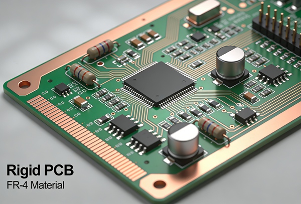
In the world of hardware engineering, a schematic is a plan, but the PCB layout is the reality. Whether you are designing a simple breakout board or a complex multi-layer system, the physical arrangement of traces determines whether your device thrives or fails due to EMI, crosstalk, or thermal runaway.
At Han-Sphere, we’ve seen how minor routing oversights can lead to costly re-spins. This guide breaks down the “golden rules” of rigid PCB layout to ensure your first prototype is your final one.
1. The Foundation: Component Placement
Before a single trace is drawn, placement dictates your routing success.
- Group by Function: Keep analog, digital, and power sections isolated to prevent noise coupling.
- Shortest Paths: Place decoupling capacitors as close as possible to the IC power pins.
- Thermal Logic: High-heat components (like MOSFETs or processors) should be centered or placed near heatsinks, away from temperature-sensitive electrolytic capacitors.
2. Critical Routing Constraints
To maintain signal integrity, follow these three pillars:
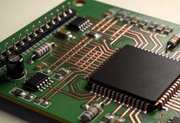
Trace Width and Spacing
Current capacity dictates width. Use a trace width calculator for power rails, ensuring they can handle the expected amperage without exceeding a 10°C temperature rise. For signal lines, maintain a minimum “3W” spacing (three times the trace width) to minimize crosstalk.
3-Way Rule for Vias
Vias introduce inductance. While necessary, over-using them on high-speed lines can degrade signal quality.
Pro Tip: Avoid placing vias directly on SMT pads (unless using VIPPO technology) as it can cause “solder thieving” during assembly.
Impedance Control
For USB, Ethernet, or HDMI interfaces, trace geometry must be calculated to match specific differential impedance (e.g., 90Ω or 100Ω).
How to Route a Rigid PCB for Maximum Stability
Follow this step-by-step workflow used by professional layout engineers.
- Define the Layer Stackup
Determine your signal and plane layers. Always aim for a symmetrical stackup to prevent board warping (bow and twist) during reflow.
- Route the “Critical Path” First
Start with high-speed interfaces (DDR, PCIe) and sensitive analog signals. These require the most direct paths and specific shielding.
- Establish the Power Grid
Route power traces wide. Use solid ground planes on adjacent layers to provide a low-impedance return path.
- Clean Up the “Spaghetti”
Once critical nets are in, route the remaining low-speed GPIOs.
- Run DRC (Design Rule Check)
Never skip this. Ensure your layout matches your manufacturer’s specific tolerances for clearance and drill sizes.
Conclusion
Rigid PCB layout and routing rules directly affect signal integrity, EMI, and manufacturability. Applying disciplined layout principles leads to stable, reliable, and cost-effective PCB designs.
This article forms the execution core of the Rigid PCB Design content cluster.
FAQ – Rigid PCB Layout & Routing
A: Right angles can cause “acid traps” during the etching process and create impedance discontinuities. While modern fabrication has improved, 45-degree miters remain the industry standard for better signal flow and manufacturing yield.
A: Generally, maintain at least 0.5mm (20 mils) of clearance. This prevents copper exposure or shorts during the board v-scoring or routing process.
A: For most modern rigid PCBs, a continuous, unbroken ground plane is superior. It provides the lowest possible inductance and the best EMI protection compared to star grounding.
Final Review Before Fabrication
Before sending your files to Han-Sphere Production, perform a final “sanity check”:
- Check for “Dead Copper” (islands that aren’t grounded).
- Ensure silkscreen text is legible and doesn’t overlap pads.
- Verify that your drill file matches your via sizes.
Ready to start your next project? Check out our PCB Manufacturing Capabilities to see how we can bring your layout to life.