A PCB can look perfect and still fail electrically.
Good manufacturing is not just about fabrication—it’s about verification.
That’s why PCB testing exists.
Whether the board is used in consumer electronics, industrial systems, automotive, or medical equipment, testing is what catches problems before products reach the field.
Typical issues found during testing include:
- open circuits
- shorts
- solder defects
- missing components
- hidden BGA failures
- functional problems
Different tests are used for different risks.
Why PCB Testing Matters
Even with a stable manufacturing process, variation still happens.
Small defects can cause:
- intermittent failures
- reduced reliability
- field returns
- costly recalls
Testing helps verify:
- electrical continuity
- solder quality
- assembly accuracy
- overall functionality
For production quality considerations, see High-Speed PCB Design for Manufacturing & Yield.
Common PCB Testing Methods
There is no single “best” test.
Manufacturers usually combine multiple methods.
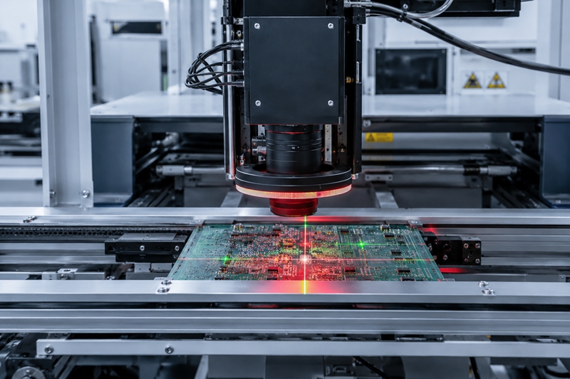
Automated Optical Inspection (AOI)
AOI uses cameras to inspect PCB assemblies automatically.
It checks for:
- missing components
- polarity errors
- solder bridging
- placement misalignment
Where AOI Works Best
- SMT assembly lines
- high-volume production
- visible solder joints
Limitations
AOI cannot inspect hidden joints, such as:
- BGA solder balls
- bottom-side hidden defects
AOI is usually one of the earliest inspection steps.
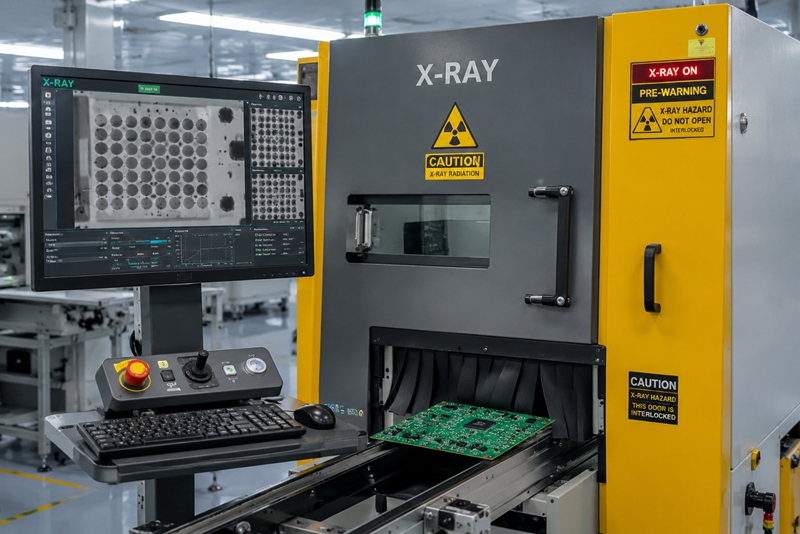
X-Ray Inspection
Some defects cannot be seen optically.
That’s where X-ray inspection comes in.
It is commonly used for:
- BGA packages
- QFN components
- hidden solder joints
X-ray can reveal:
- voids
- cold solder joints
- insufficient solder
- bridging under components
For complex assemblies, X-ray is often mandatory.
In-Circuit Testing (ICT)
ICT electrically checks individual components on the board.
Typical checks include:
- shorts
- opens
- resistance
- capacitance
- component values
Advantages
- fast testing
- high coverage
- suitable for volume production
Limitation
ICT often requires a dedicated fixture.
That increases upfront cost.
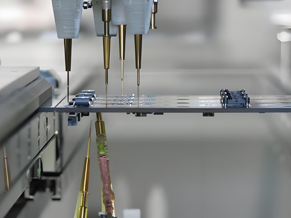
Flying Probe Testing
Flying probe testing is similar to ICT but without a custom fixture.
Instead, moving probes contact test points automatically.
Best For
- prototypes
- low-volume production
- quick-turn manufacturing
Trade-Off
Slower than ICT, but more flexible.
This is why many PCB prototypes use flying probe testing first.
Functional Testing (FCT)
Functional testing verifies whether the assembled PCB actually works.
Instead of checking isolated components, it tests:
“Does the board perform its intended function?”
Examples:
- power-up testing
- communication verification
- signal measurement
- software interaction
Functional testing is often the final validation step.
Burn-In Testing
For high-reliability applications, boards may undergo burn-in testing.
The board runs under:
- elevated temperature
- continuous operation
- electrical load
Purpose:
- expose early-life failures
- improve reliability confidence
Common in:
- aerospace
- automotive
- industrial electronics
Boundary Scan (JTAG) Testing
For dense PCBs with limited probe access, boundary scan becomes useful.
It allows electrical testing through IC interfaces without physical probing.
Especially useful for:
- complex digital systems
- fine-pitch components
- multilayer boards
PCB Testing Method Comparison
| Method | Best For | Main Purpose | Limitation |
|---|---|---|---|
| AOI | SMT inspection | visual defects | hidden joints |
| X-Ray | BGA/QFN | hidden solder | higher cost |
| ICT | mass production | electrical checks | fixture required |
| Flying Probe | prototype | electrical testing | slower |
| Functional Test | final validation | real operation | custom setup |
| Burn-In | reliability | stress testing | time-consuming |
How to Choose the Right PCB Testing Method
Testing strategy depends on:
- product complexity
- production volume
- reliability requirement
- budget
Prototype Stage
Recommended:
- flying probe
- AOI
- functional test
Mid-Volume Production
Recommended:
- AOI
- ICT or flying probe
- functional testing
High-Reliability Products
Recommended:
- X-ray
- ICT
- functional testing
- burn-in testing
How to Improve PCB Testability
Good testing starts in the design stage.
- 1. Add Test Points
Without access points:
. ICT becomes difficult
. debugging slows down - 2. Consider Component Spacing
Overly dense layouts reduce probe accessibility.
- 3. Design for DFM and DFA
Manufacturability affects testing success.
Related reading:
High-Speed PCB Design for Manufacturing & Yield
PCB Design Review Checklist - 4. Plan Testing Early
Testing should not be added at the end.
Include it during:
. schematic stage
. layout planning
. assembly review
Common PCB Testing Mistakes
Typical problems seen in production:
- skipping functional testing
- relying only on visual inspection
- poor test-point access
- no X-ray for BGA assemblies
- testing added too late in the project
Practical Notes from Real Production
What usually happens in practice:
- prototypes often use flying probe + manual debugging
- mass production shifts to ICT for speed
- BGA assemblies almost always require X-ray inspection
- functional testing catches issues electrical tests miss
No single test catches everything.
The best strategy combines multiple methods.
Conclusion
PCB testing is essential for ensuring quality, reliability, and manufacturing consistency.
Different methods serve different purposes—AOI for visual defects, ICT and flying probe for electrical verification, X-ray for hidden solder joints, and functional testing for real-world performance.
Choosing the right mix of testing methods depends on product complexity, production volume, and reliability requirements.