In the electronics manufacturing industry, the terms PCB and PCBA are thrown around constantly. To an outsider, they sound like minor acronym variations. However, to a hardware designer, procurement officer, or manufacturing facility, they represent two completely different stages of a product’s lifecycle, involving distinct supply chains, engineering skill sets, and cost structures.
Misunderstanding the boundaries between a bare board and a completed assembly can lead to communication errors, delayed quotes, and logistical bottlenecks.
In this factory-grade guide, HanSphere breaks down the exact technical, mechanical, and economic differences between a PCB and a PCBA, helping you streamline your next hardware build.
1. Core Definitions: The Fundamental Difference
To understand how these two elements interact, we must establish their baseline definitions:
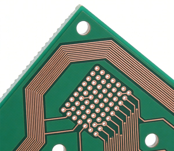
- PCB (Printed Circuit Board): This is the raw, unpopulated foundation. It is a mechanical structure consisting of insulating fiberglass layers laminated with conductive copper pathways. It contains pads, traces, through-holes, and a protective solder mask, but it houses zero components. It conducts no logic on its own; it is an empty highway network waiting for traffic.
- Deep Dive: Read our introductory guide to learn more about layers and core substrates in What is a PCB?.
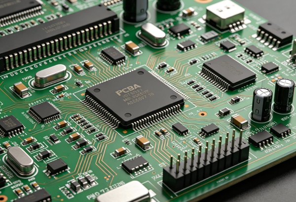
- PCBA (Printed Circuit Board Assembly): This is the fully populated, functioning circuit. It is the bare PCB after it has passed through production lines to have all its active and passive components—such as microcontrollers, resistors, connectors, and power chips—permanently soldered into place. It is a live, operational system ready to be powered up.
- Deep Dive: Explore our breakdown of production models and testing workflows in What is PCBA?.
2. Side-by-Side Comparison Matrix
To give your procurement or engineering team an immediate macro-view, here is how the two stages stack up against each other across critical operational metrics:
| Operational Metric | PCB (Bare Board) | PCBA (Assembled Board) |
| Physical Status | Empty, unpopulated fiberglass sheet. | Fully loaded board with active/passive components. |
| Primary Goal | To provide mechanical support and electrical paths. | To execute the device’s programmed electronic logic. |
| Required Input Files | Gerber files (RS-274X or ODB++), Drill data. | Gerber files + Bill of Materials (BOM) + Centroid (Pick & Place) file. |
| Primary Technologies | Photolithography, Etching, Drilling, Plating. | SMT Reflow Soldering, THT Wave/Selective Soldering. |
| Design Optimization Focus | DFM (Design for Manufacturing – trace/space clearances). | DFA (Design for Assembly – component orientations). |
| Testing Protocols | E-Test (Flying Probe or Bed-of-Nails for continuity). | AOI, X-Ray (AXI), ICT, and Functional Testing (FCT). |
| Cost Composition | Dominated by board size, layer count, and raw materials. | Dominated by electronic component costs and machine setup labor. |
3. Technical Walkthrough: How One Becomes the Other
The transition from a raw PCB to a functioning PCBA is where complex automation takes over. This process happens entirely within specialized electronic contract manufacturing facilities.
Fabrication: The factory builds the raw PCB using advanced copper etching and multi-layer pressing techniques.
Solder Paste Application: In the PCBA phase, a stencil prints solder paste precisely onto the bare PCB pads.
Component Mounting: Automated robotic arms mount components onto the board. Depending on your design, this will leverage ultra-fast surface mount systems, traditional through-hole setups, or a hybrid approach.
- Internal Link: See which method fits your product requirements by reviewing our comparison of SMT vs. THT Assembly.
Soldering & Solidification: The board enters high-temperature ovens to fuse the components permanently to the copper infrastructure.
4. Engineering Standards: DFM vs. DFA
The difference between PCB and PCBA dictates how an engineer must optimize their CAD layout designs before sending them to the HanSphere facility.
Designing the Bare PCB: Focus on DFM
When designing a bare PCB, your goal is to ensure the fabrication house can physically etch and drill the board with a high yield. You must optimize for Design for Manufacturing (DFM) rules, focusing on minimum trace widths, via annular rings, and copper balance to prevent warpage.
- Internal Link: Review our factory floor metrics in our PCB Design for Manufacturing (DFM) Guide.
Designing the PCBA: Focus on DFA
When preparing for assembly, you must shift your focus to Design for Assembly (DFA). This involves positioning parts so that automated nozzles can grab them without hitting neighboring components, ensuring correct component polarities, and optimizing pad sizes to prevent parts from shifting during reflow.
- Internal Link: For specialized layouts, make sure to follow our strict Rigid-Flex PCB Design Guidelines.
5. Procurement and Supply Chain Realities
From a purchasing perspective, the budget allocation and timeline management for PCBs and PCBAs are starkly different.
- PCB Sourcing: This is a localized raw material purchase. Your lead times are highly predictable, influenced mainly by the number of layers and your chosen surface finish (e.g., HASL vs. ENIG).
- PCBA Sourcing: This is a complex global logistics operation. The timeline of a PCBA is completely dependent on the single component with the longest lead time in your Bill of Materials (BOM). If a specific microcontroller faces a global shortage, your entire assembly line is placed on hold, even if the bare PCBs are already sitting on the factory floor.
HanSphere Factory Insight: To mitigate supply chain friction, we highly recommend utilizing our Turnkey PCBA model. By letting HanSphere manufacture the board and source components simultaneously from verified global vendors, you eliminate double-shipping costs and minimize communication delays.
6. FAQ: PCB vs. PCBA Clarity
A: Yes, minor trace damage on external layers can sometimes be repaired using conductive epoxy or jumper wires, but it compromises aesthetics and long-term reliability. At HanSphere, every bare board undergoes strict Electrical Testing (E-Test) to ensure zero open or short circuits before it ever reaches assembly.
A: Absolutely. This is known as Consigned or Kitted Assembly. However, ensure your components are delivered in proper tape-and-reel packaging with explicit overage counts so our automated high-speed SMT machines don’t run out during placement.
A: No. A PCBA is strictly the populated circuit board. Putting the PCBA inside a plastic or metal housing along with user interfaces and wire harnesses is called Box-Build Assembly or Final System Integration, which HanSphere also provides as part of our extended end-to-end services.