In electronic manufacturing, people often use the terms PCB and PCBA interchangeably. However, they are entirely different stages of the hardware development cycle. If you order a PCB, you receive a flat, green piece of fiberglass. If you order a PCBA, you receive the fully functioning electronic “brain” of your product.
In this guide, HanSphere demystifies what a PCBA is, how the assembly process works step-by-step, and how to choose the right sourcing strategy for your hardware project.
1. PCB vs. PCBA: What is the Difference?
To put it simply:
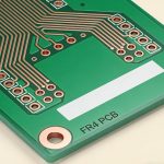
- PCB (Printed Circuit Board): The raw, unpopulated board. It contains copper pathways (traces) and insulation layers but has zero electronic components soldered onto it. It cannot function on its own.
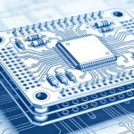
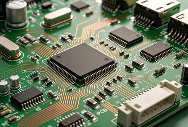
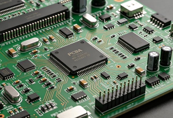
- PCBA (Printed Circuit Board Assembly): The completed board after all active and passive components—such as microchips, resistors, capacitors, and connectors—have been permanently soldered onto it. A PCBA is a fully operational electronic circuit.
Analogy: Think of a PCB as the concrete foundation and frame of an empty house. A PCBA is that same house completely furnished, wired with electricity, and ready for you to move in.
2. The 3 Main Component Sourcing Models for PCBA
When you partner with a manufacturer like HanSphere for assembly, you can choose how your components are sourced:
- 1. Turnkey PCBA (Recommended): The factory handles everything. HanSphere manufactures the bare PCB, sources all components from authorized global distributors (like DigiKey, Mouser, or Arrow), and completes the assembly. This model saves you shipping costs, minimizes communication friction, and reduces lead times.
- 2. Consigned / Kitted PCBA: You source and ship all components directly to our factory floor. HanSphere is strictly responsible for the assembly labor.
- 3. Partial Turnkey / Hybrid: You provide the proprietary microchips or specialized connectors, and HanSphere sources the standard passive components (resistors, capacitors, diodes).
3. How a PCBA is Made: The Step-by-Step Assembly Process
The journey of turning a bare board into a working assembly involves ultra-precise automation. Here is how we do it on the HanSphere factory lines:
- Step 1: Design for Assembly (DFA) Review
Before production starts, our CAM engineers check your Bill of Materials (BOM) and Gerber files to identify footprints or clearance issues that could disrupt automated machinery.
- Step 2: Solder Paste Printing
A laser-cut stainless steel stencil is aligned perfectly over the bare PCB. Solder paste is then swept across the stencil, depositing precise amounts of paste only onto the component pads.
- Step 3: High-Speed Component Placement (SMT)
Automated pick-and-place robotic nozzles rapidly lift components from tape reels and place them onto the sticky solder paste with micrometer precision.
Internal Link: To see the inner workings of this automation, check out our Complete SMT Assembly Guide. - Step 4: Reflow Soldering
The populated boards travel through a conveyorized oven. The temperature ramps up to melt the solder paste, then cools down to form solid, reliable permanent bonds.
- Step 5: Through-Hole Insertion & Wave Soldering (If needed)
If your board requires heavy-duty parts like bulk transformers or screw terminals, they are inserted into drilled holes and soldered using automated wave or selective soldering equipment.
Internal Link: Learn more about this mechanical bonding technique in our Through-Hole Technology (THT) Assembly Guide. - Step 6: Multi-Stage Inspection & Quality Testing
We deploy multiple testing phases to guarantee perfect functionality:
. AOI (Automated Optical Inspection): Scans for missing or misaligned parts.
. AXI (Automated X-Ray Inspection): Peers underneath dense BGA chips to verify hidden solder connections.
. FCT (Functional Testing): Powering on the board to simulate its real-world operation.
FAQ: Common PCBA Questions
A: Yes. For a bare PCB, you only need Gerber or ODB++ files. For a PCBA, you must also provide a BOM (Bill of Materials) listing all parts, and a Centroid/Pick-and-Place file that tells our machines the exact X-Y coordinates and rotation of every component.
A: A cold solder joint happens when the solder doesn’t melt completely, creating a loose or intermittent connection. We prevent this by carefully calibrating our reflow oven thermal profiles based on the board’s copper thickness and layer count.
A: Absolutely. HanSphere provides rapid PCBA prototyping services with no minimum order quantity (MOQ) to help you test and perfect your design before moving to mass production.