Look around you. Your smartphone, your laptop, the smart coffee maker in your kitchen, and even the dashboard of your car all have one crucial thing in common: they rely on a PCB (Printed Circuit Board) to function.
But what exactly is a PCB? How does it work, and why is it the foundation of modern electronics?
In this comprehensive guide, HanSphere breaks down everything you need to know about Printed Circuit Boards, from their basic structure to how they are manufactured on our factory floor.
1. What Does a PCB Actually Do?
At its core, a Printed Circuit Board (PCB) is a rigid, non-conductive structure that hosts and connects electronic components.
Before PCBs were invented, circuits were built using point-to-point wiring. Engineers manually soldered wires directly between components. This was messy, fragile, took up massive amounts of space, and was impossible to mass-produce.
A PCB solves this by “printing” copper pathways (called traces) onto an insulating board. This allows components like resistors, chips, and capacitors to securely connect and communicate with each other in a compact, reliable, and highly repeatable setup.
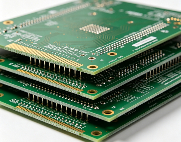
2. Anatomy of a PCB: The 4 Main Layers
If you look at a cross-section of a standard PCB, it looks like a multi-layered sandwich. Each layer serves a unique purpose:
1. The Substrate (FR-4 Core)
The base material, or backbone, of the PCB. It is usually made of fiberglass, with FR-4 (Flame Retardant 4) being the industry standard. It provides the mechanical rigidity and electrical insulation for the board.
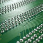
2. The Copper Layer
Laminated onto the substrate with heat and adhesive. This is where the magic happens. The copper is chemically etched away to leave behind the fine lines (traces) that carry electrical signals across the board.
- Note: A board can be single-sided (one copper layer), double-sided (two layers), or multi-layered (up to 30+ layers).
3. The Solder Mask
The layer that gives PCBs their iconic color (traditionally green, though HanSphere also offers blue, black, white, and red). It is a protective polymer coating applied over the copper to prevent accidental short circuits, oxidation, and solder bridges during assembly.
4. The Silkscreen
The top layer of human-readable text. It prints white (or contrasting color) letters, numbers, and symbols onto the board. This helps engineers and assembly machines identify component locations, polarity, and logos (like your custom HanSphere stamp).
3. Common Types of PCBs
Depending on your project’s mechanical and electrical needs, PCBs come in various formats:
- Rigid PCBs: The most common type. They are solid and cannot bend (e.g., computer motherboards).
- Flex PCBs: Made of flexible plastics (like Polyimide). They can twist and bend to fit into tight or kinetic spaces (e.g., camera hinges, medical wearables).
- Rigid-Flex PCBs: A hybrid combination of both, offering the strength of rigid boards and the space-saving benefits of flex.
- HDI PCBs (High-Density Interconnect): Feature higher wiring density per unit area, using microvias to handle advanced microchips.

4. How is a PCB Made? [The Quick Lifecycle]
Step 1: Design & DRC
An engineer creates the blueprint in CAD software (like Altium or KiCad) and submits it to a factory. At HanSphere, our CAM team performs a free DRC (Design Rule Check) to ensure the design can be manufactured without errors.
Step 2: Fabrication
The raw fiberglass sheet is clad in copper, exposed to UV light through a film, and etched. Holes are drilled, copper is electroplated inside those holes to connect layers, and the solder mask is applied.
Step 3: Assembly (PCBA)
The bare board is populated with electronic components using automated high-speed SMT (Surface Mount) or THT (Through-Hole) assembly lines.
Internal Link: Curious about how we attach components? Check out our Ultimate SMT vs. THT Assembly Comparison Guide.
FAQ: PCB Basics for Beginners
A: A PCB is the empty, bare circuit board with no parts attached. A PCBA (Printed Circuit Board Assembly) is the final, fully functional board with all the chips and components soldered onto it.
A: Absolutely. While green is standard because it is highly visible for inspection, HanSphere offers black, matte black, blue, red, yellow, and white solder masks to match your branding.
A: Right here! HanSphere specializes in both fast-turn PCB prototyping and mass production.