In PCB assembly, defects are cheaper to catch early.
A missing resistor after reflow is easy to fix.
A defective board found after final assembly is not.
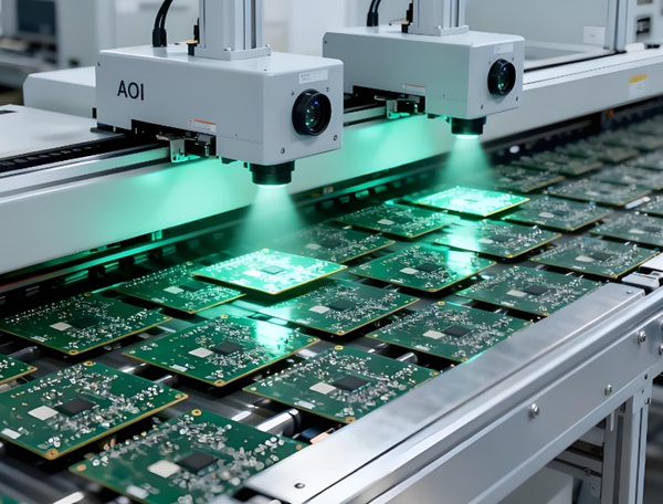
That’s why AOI (Automated Optical Inspection) is used in almost every SMT production line.
AOI is fast, repeatable, and scalable. It catches many common assembly defects before they become expensive failures later in production.
But it also has limitations—and understanding both sides matters.
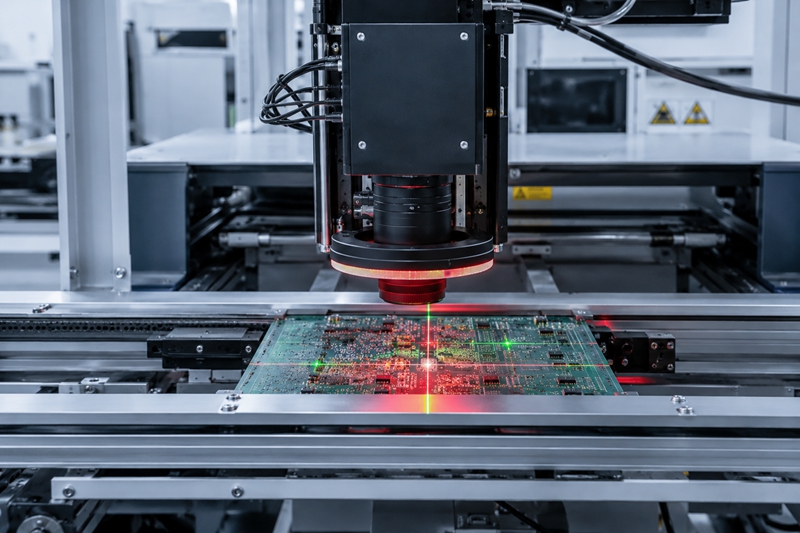
What Is AOI Inspection?
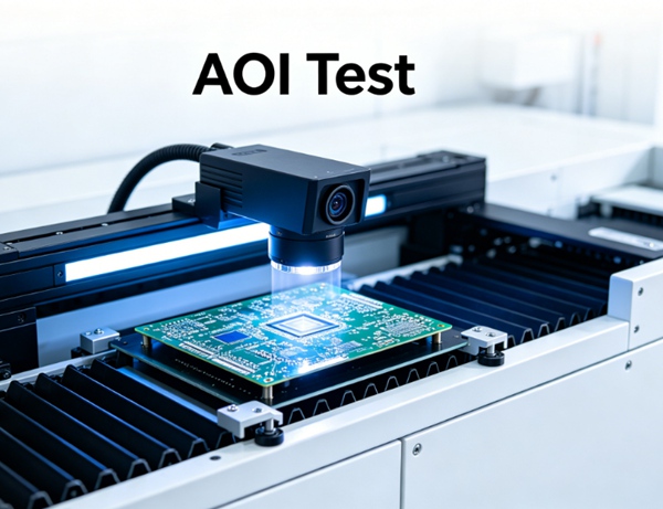
AOI stands for Automated Optical Inspection.
It uses:
- high-resolution cameras
- image processing software
- comparison algorithms
to inspect PCB assemblies automatically.
The system compares the assembled board against:
- CAD data
- Gerber files
- golden reference images
and flags abnormalities.
In practice, AOI is mainly used to identify:
“Does the board visually look assembled correctly?”
Where AOI Is Used in PCB Assembly
AOI is commonly used at multiple stages.
Pre-Reflow AOI
Performed before solder reflow.
Checks:
- solder paste deposition
- component placement accuracy
- polarity orientation
Purpose:
- catch mistakes early before soldering
Post-Reflow AOI
Performed after soldering.
Checks:
- solder quality
- tombstoning
- missing components
- bridging defects
This is the most common AOI stage.
What Defects Can AOI Detect?
AOI is especially good at visible defects.
1. Missing Components
The system detects:
- absent resistors
- missing ICs
- incomplete assembly
One of the most common findings.
2. Wrong Component Placement
AOI identifies:
- shifted parts
- skewed placement
- rotation errors
Even small placement offsets can affect reliability.
3. Polarity Errors
For polarized components such as:
- diodes
- electrolytic capacitors
- LEDs
- IC orientation
AOI checks whether direction is correct.
4. Solder Bridges
Excess solder can create shorts between pins.
AOI is effective at detecting:
- visible bridging
- solder overflow
Especially on fine-pitch devices.
5. Tombstoning
Small passive components sometimes stand upright during reflow.
AOI easily detects these failures.
Common with:
- 0201
- 0402 components
6. Insufficient or Excessive Solder
AOI evaluates solder joint appearance and shape.
But accuracy depends on:
- lighting
- viewing angle
- programming quality
What AOI Cannot Detect Well
AOI is powerful—but not perfect.
Its biggest limitation:
it can only inspect what the camera can see.
Problems AOI struggles with:
Hidden Solder Joints
Especially:
- BGA packages
- QFN components
The solder is underneath the component.
This is where X-ray inspection becomes necessary.
Future related topic: PCB X-Ray Inspection for BGA and Hidden Solder Joints
Internal Cracks
AOI cannot see:
- internal solder fractures
- voids
- barrel defects
Electrical Failures
A board may look perfect visually but still fail electrically.
That’s why AOI is often combined with:
- ICT
- flying probe testing
- functional testing
More here: PCB Testing Methods Explained
AOI vs Manual Inspection
| Method | AOI | Manual Inspection |
|---|---|---|
| speed | fast | slow |
| consistency | high | operator dependent |
| scalability | excellent | limited |
| hidden defects | poor | poor |
In modern production:
AOI supplements operators—it doesn’t fully replace them.
AOI in High-Volume Production
AOI becomes especially valuable when:
- production volume is high
- repeatability matters
- defect escape cost is expensive
Advantages:
- early defect detection
- lower rework cost
- improved production yield
Related: High-Speed PCB Design for Manufacturing & Yield
How to Improve AOI Inspection Results
Good inspection starts with good design.
- 1. Maintain Clear Component Spacing
Dense layouts make optical inspection harder.
- 2. Use Consistent Silkscreen Marking
Helps identify orientation.
- 3. Follow DFM Guidelines
Better manufacturability improves inspection reliability.
- 4. Optimize Lighting and Programming
False positives often come from poor AOI programming.
A well-tuned AOI program matters as much as hardware.
Common AOI Mistakes
Typical production issues:
- relying only on AOI
- poor golden board reference
- excessive false alarms
- skipping post-reflow inspection
- using AOI for hidden-joint verification
AOI is powerful—but it is not the entire quality process.
Practical Notes from Real Production
What often happens in real factories:
- AOI catches placement errors surprisingly well
- most false rejects come from poor programming
- BGA defects almost always need X-ray follow-up
- post-reflow AOI is more valuable than pre-reflow in many cases
The best results come from combining AOI with electrical testing.
Conclusion
AOI inspection is one of the most important quality control methods in PCB assembly.
It helps detect common visual defects quickly and consistently, improving manufacturing yield and reducing costly failures later in production.
However, AOI has limitations—especially for hidden solder joints and electrical failures—so it works best as part of a broader testing strategy.
FAQ
A: AOI stands for Automated Optical Inspection, used to visually inspect PCB assemblies for defects.
A: Missing components, polarity errors, solder bridges, placement issues, and tombstoning.
A: No. Hidden joints usually require X-ray inspection.
A: AOI is faster and more consistent, but manual inspection is still useful for verification.
A: Usually before reflow (pre-reflow) and after soldering (post-reflow).