A board can pass AOI and still fail.
That happens more often than people expect.
The reason is simple:
cameras only see what is visible.
Once solder joints move underneath components, optical inspection becomes limited.
That’s where X-ray inspection comes in.
For assemblies using:
- BGA
- QFN
- LGA
- hidden solder pads
X-ray inspection is often the only practical way to verify solder quality.
What Is PCB X-Ray Inspection?
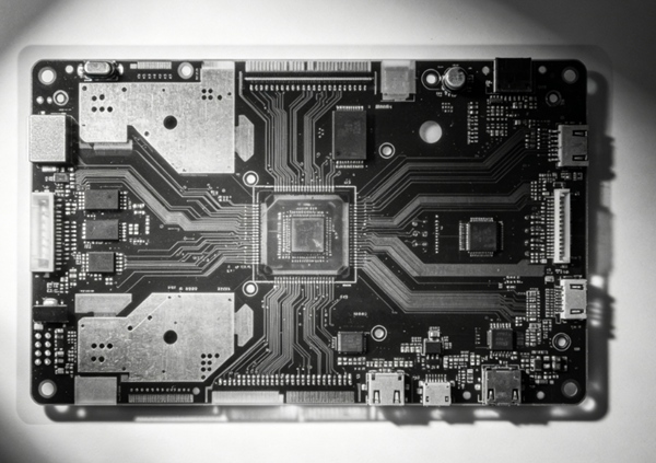
X-ray inspection uses X-ray imaging to look inside PCB assemblies without damaging the board.
Instead of surface images, it shows:
- solder joint quality
- internal connections
- hidden defects
The result is a grayscale image where solder density becomes visible.
This makes it possible to inspect areas that AOI cannot access.
Related reading: AOI Inspection in PCB Assembly: What Can It Detect?
Why X-Ray Inspection Is Important
Modern PCB assemblies continue to become:
- smaller
- denser
- more complex
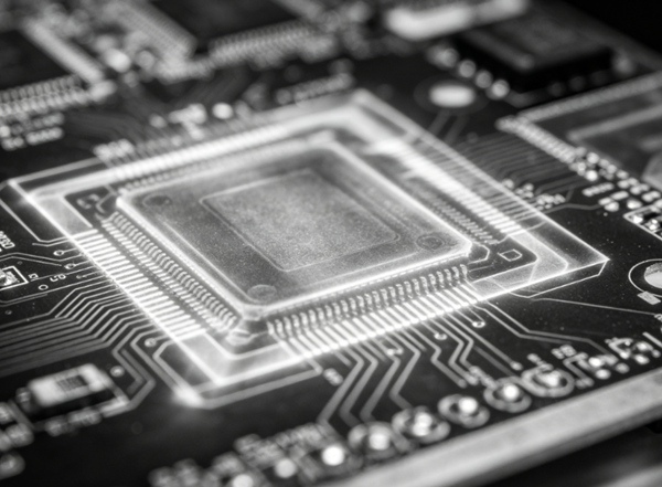
Many packages now hide solder joints underneath the component body.
Without X-ray:
- solder bridges may go unnoticed
- voids remain invisible
- opens and shorts become harder to identify
For high-reliability products, skipping X-ray can increase field failure risk.
Components That Usually Require X-Ray Inspection
BGA (Ball Grid Array)
The most common use case.
Because solder balls sit under the package:
- optical inspection cannot see them
- electrical testing alone may miss marginal joints
X-ray verifies:
- ball alignment
- solder consistency
- bridging
QFN (Quad Flat No-Lead)
QFN packages often include hidden center pads.
Common problems:
- poor wetting
- insufficient solder
- voiding
LGA Packages
Land Grid Array devices also benefit from X-ray verification.
Especially in:
- RF systems
- automotive electronics
Dense SMT Assemblies
High-density layouts may block visual access, even for visible leads.
Common Defects X-Ray Can Detect
1. Solder Voids
Voids are trapped air pockets inside solder joints.
Small voids are usually acceptable.
Excessive voiding can affect:
- thermal performance
- reliability
- mechanical strength
Especially critical in:
- power electronics
- thermal pads
2. Solder Bridges
Hidden short circuits between pads.
Particularly common in:
- fine-pitch BGA
- dense routing areas
3. Open Solder Joints
Incomplete solder connections.
Can result in:
- intermittent failures
- unstable operation
4. Misalignment
Components may shift slightly during reflow.
X-ray shows whether solder balls align properly.
5. Insufficient or Excessive Solder
Uneven solder distribution becomes visible in X-ray images.
2D vs 3D X-Ray Inspection
2D X-Ray
Most common approach.
Advantages:
- faster
- lower cost
- suitable for production screening
3D CT X-Ray (Computed Tomography)
Provides cross-sectional imaging.
Advantages:
- deeper failure analysis
- internal layer visibility
Typically used for:
- failure investigation
- high-end applications
Related topic: PCB Failure Analysis
X-Ray vs AOI (Quick Comparison)
| Feature | AOI | X-Ray |
|---|---|---|
| visible solder joints | excellent | good |
| hidden solder joints | poor | excellent |
| BGA inspection | limited | strong |
| speed | faster | slower |
| cost | lower | higher |
In practice:
AOI and X-ray complement each other.
They are not substitutes.
When Is X-Ray Inspection Necessary?
Not every board needs it.
Usually Recommended For
- BGA assemblies
- QFN packages
- automotive electronics
- aerospace systems
- medical devices
- high-density SMT boards
Less Critical For
- simple through-hole boards
- low-density consumer products
How to Improve X-Ray Inspection Results
- 1. Design for Manufacturability (DFM)
Good pad design improves solder consistency.
- 2. Optimize Stencil Design
Proper solder paste volume reduces defects.
- 3. Control Reflow Profile
Temperature profile strongly affects solder quality.
- 4. Use X-Ray Early in NPI
During new product introduction:
. verify process stability
. identify hidden defects early
Common X-Ray Inspection Mistakes
Typical production problems:
- relying only on AOI for BGAs
- ignoring solder void percentages
- skipping X-ray during NPI
- using poor image interpretation standards
X-ray only works when inspection criteria are consistent.
Practical Notes from Real Production
What often happens in factories:
- BGA bridges are usually found with X-ray, not AOI
- many intermittent failures trace back to hidden solder issues
- voiding becomes a major concern in power electronics
- X-ray is most valuable during early production builds
For mature products, sampling inspection is often used instead of 100% inspection.
Conclusion
PCB X-ray inspection plays a critical role in verifying hidden solder joints and ensuring assembly quality.
For BGA, QFN, and high-density PCB assemblies, it helps identify defects that optical inspection cannot detect. While it adds cost, it significantly reduces the risk of hidden failures in high-reliability products.
FAQ
A: Because many solder joints are hidden underneath components and cannot be inspected visually.
A: No. AOI cannot inspect hidden solder joints like BGA balls.
A: Voids, solder bridges, opens, misalignment, and solder distribution problems.
A: No. It is mainly used for complex SMT assemblies and hidden solder packages.
A: 2D is faster and common for production, while 3D CT provides deeper internal analysis.