Плата может пройти AOI и все равно провалиться.
Это случается чаще, чем люди ожидают.
Причина проста:
Камеры видят только то, что видно.
Как только паяные соединения перемещаются под компоненты, оптический контроль становится ограниченным.
Именно здесь Рентгеновский контроль входит.
Для сборок с использованием:
- BGA
- QFN
- LGA
- скрытые паяльные площадки
Рентгеновский контроль часто является единственным практическим способом проверки качества припоя.
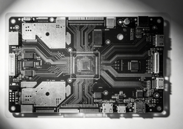
Что такое рентгеновский контроль печатных плат?
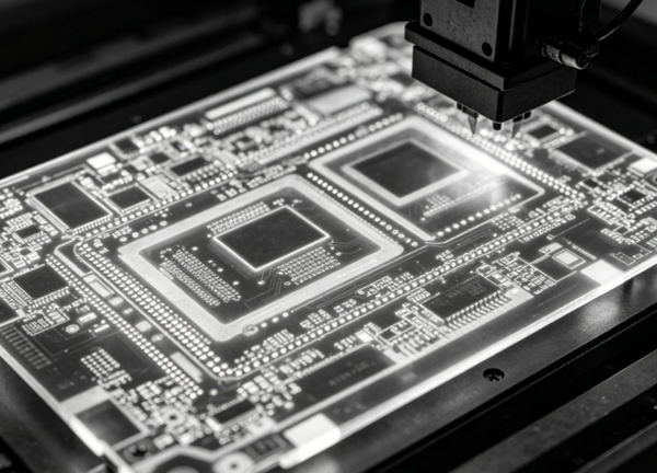
При рентгеновском контроле используется рентгеновское изображение, позволяющее заглянуть внутрь узлов печатной платы, не повреждая ее.
Вместо поверхностных изображений на нем изображены:
- качество паяного соединения
- внутренние соединения
- скрытые дефекты
В результате получается полутоновое изображение, на котором видна плотность припоя.
Это позволяет исследовать области, к которым AOI не имеет доступа.
Похожие статьи: Контроль AOI при сборке печатных плат: Что он может обнаружить?
Почему важен рентгеновский контроль
Современные сборки печатных плат продолжают становиться все более совершенными:
- меньше
- плотнее
- более сложный
Многие корпуса теперь скрывают паяные соединения под корпусом компонента.
Без рентгена:
- Мостики припоя могут остаться незамеченными
- Пустоты остаются невидимыми
- Открытия и шорты становится сложнее идентифицировать
Для высоконадежных изделий пропуск рентгена может увеличить риск отказа в полевых условиях.
Компоненты, которые обычно требуют рентгеновского контроля
BGA (Ball Grid Array)
Самый распространенный вариант использования.
Потому что шарики припоя находятся под упаковкой:
- оптический контроль не может их увидеть
- При проведении только электрических испытаний можно пропустить дефектные соединения
Рентген подтверждает:
- центровка шара
- консистенция припоя
- наведение мостов
QFN (Quad Flat No-Lead)
Корпуса QFN часто содержат скрытые центральные площадки.
Общие проблемы:
- плохое смачивание
- недостаточное количество припоя
- аннулирование
Пакеты LGA
Устройства Land Grid Array также выигрывают от рентгеновской проверки.
Особенно в:
- Радиочастотные системы
- автомобильная электроника
Плотные SMT-сборки
Высокая плотность застройки может блокировать визуальный доступ даже к заметным проводам.

Распространенные дефекты, выявляемые с помощью рентгена
1. Пустоты в припое
Пустоты - это воздушные карманы внутри паяных соединений.
Небольшие пустоты обычно допустимы.
Чрезмерное мочеиспускание может повлиять на состояние организма:
- тепловые характеристики
- надежность
- механическая прочность
Особенно критично в:
- силовая электроника
- термопрокладки
2. Паяльные мостики
Скрытые короткие замыкания между колодками.
Особенно часто встречается в:
- BGA с мелким шагом
- плотные зоны маршрутизации
3. Открытые паяные соединения
Неполное паяное соединение.
Может привести к:
- периодические сбои
- нестабильная работа
4. Несоответствие
Компоненты могут немного сместиться во время расплавления.
Рентгеновский снимок показывает, правильно ли выровнены шарики припоя.
5. Недостаточное или избыточное количество припоя
Неравномерное распределение припоя становится заметным на рентгеновских снимках.
Двухмерный и трехмерный рентгеновский контроль
Двухмерный рентген
Самый распространенный подход.
Преимущества:
- быстрее
- низкая стоимость
- подходит для производственной сортировки
3D КТ-рентген (компьютерная томография)
Обеспечивает визуализацию поперечного сечения.
Преимущества:
- более глубокий анализ отказов
- видимость внутреннего слоя
Обычно используется для:
- исследование неисправностей
- высокотехнологичные приложения
Похожие темы: Анализ отказов печатных плат
Рентгеновские лучи против AOI (краткое сравнение)
| Характеристика | AOI | Рентген |
|---|---|---|
| видимые паяные соединения | отличный | хорошо |
| скрытые паяные соединения | бедный | отличный |
| Инспекция BGA | ограниченный | сильный |
| скорость | быстрее | медленнее |
| стоимость | ниже | выше |
На практике:
AOI и рентгенография дополняют друг друга.
Они не являются заменителями.
Когда необходим рентгеновский контроль?
Не каждая доска нуждается в этом.
Обычно рекомендуется для
- Сборки BGA
- Корпуса QFN
- автомобильная электроника
- аэрокосмические системы
- медицинские приборы
- Высокоплотные SMT-платы
Менее критично для
- простые платы со сквозными отверстиями
- потребительские товары низкой плотности
Как улучшить результаты рентгеновского контроля
- 1. Проектирование для обеспечения технологичности (DFM)
Хорошая конструкция площадки улучшает консистенцию припоя.
- 2. Оптимизация дизайна трафарета
Правильный объем паяльной пасты уменьшает количество дефектов.
- 3. Управление профилем доводки
Температурный профиль сильно влияет на качество припоя.
- 4. Используйте рентгеновские снимки на ранних этапах NPI
Во время внедрения нового продукта:
. проверка стабильности процесса
. выявление скрытых дефектов на ранней стадии
Распространенные ошибки при рентгеновском обследовании
Типичные производственные проблемы:
- полагаясь только на AOI для BGA
- игнорирование процента пустот в пайке
- пропуск рентгена во время NPI
- использование плохих стандартов интерпретации изображений
Рентгенография работает только в том случае, если критерии проверки последовательны.
Практические заметки с реального производства
То, что часто происходит на заводах:
- Мосты BGA обычно обнаруживаются с помощью рентгена, а не AOI
- Многие периодические сбои связаны со скрытыми проблемами с припоем
- образование пустот становится серьезной проблемой в силовой электронике
- Рентгеновские снимки наиболее ценны на ранних этапах производства.
Для зрелых продуктов часто используется выборочный контроль вместо контроля 100%.
Заключение
Рентгеновский контроль печатных плат играет важную роль в проверке скрытых паяных соединений и обеспечении качества сборки.
При сборке BGA, QFN и печатных плат высокой плотности он помогает выявить дефекты, которые не может обнаружить оптический контроль. Хотя это и увеличивает затраты, но значительно снижает риск скрытых отказов в высоконадежных изделиях.
ЧАСТО ЗАДАВАЕМЫЕ ВОПРОСЫ
О: Потому что многие паяные соединения скрыты под компонентами и не поддаются визуальному контролю.
О: Нет. AOI не может контролировать скрытые паяные соединения, такие как шарики BGA.
A: Пустоты, мостики припоя, разрывы, несоосность и проблемы с распределением припоя.
О: Нет. В основном он используется для сложных SMT-сборок и пайки скрытым припоем.
О: 2D быстрее и привычнее для производства, а 3D КТ обеспечивает более глубокий внутренний анализ.