16 марта 2026 года
Руководство по проектированию печатных плат FR4: Структура слоев и контроль импеданса
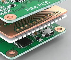
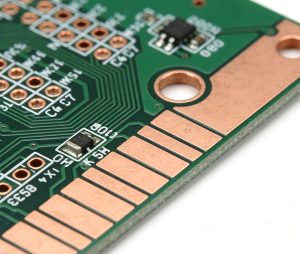
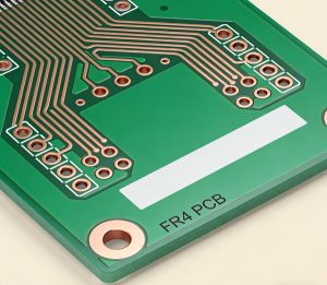
PCB stackup design defines the arrangement of copper layers and dielectric materials inside a circuit board. In FR4-based PCBs, the stackup structure determines signal integrity, impedance control, and overall mechanical stability. This article explains how FR4 PCB stackups are designed and what engineers should consider when planning multilayer boards.
Читать далее