A PCB can pass visual inspection and still fail electrically.
That’s why manufacturers rely on electrical testing after assembly.
Two of the most common methods are:
- ICT (In-Circuit Testing)
- Flying Probe Testing
Both check electrical integrity.
But they are designed for very different production situations.
In most projects, the real question is not:
“Which one is better?”
It’s:
“Which one makes sense for this production stage?”
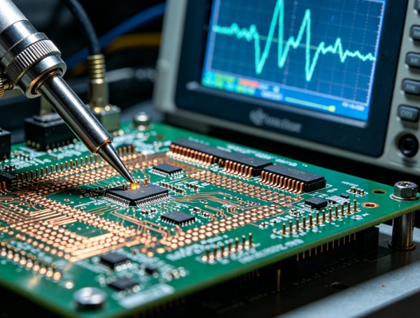
What Is ICT (In-Circuit Testing)?
ICT uses a custom test fixture—often called a bed-of-nails fixture—to contact test points on the PCB.
The system checks:
- opens
- shorts
- resistance
- capacitance
- component values
- polarity
Because multiple points are tested simultaneously, ICT is very fast.
What Is Flying Probe Testing?
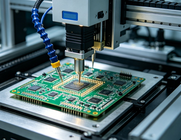
Flying probe testing performs similar electrical checks, but without a dedicated fixture.
Instead:
movable probes automatically contact test points on the PCB.
This makes it highly flexible.
Typical checks include:
- continuity
- shorts
- component verification
- polarity checks
The main difference:
no custom fixture required.
Overview: PCB Testing Methods Explained: AOI, ICT, Flying Probe, X-Ray & Functional Testing
ICT vs Flying Probe (Quick Comparison)
| Feature | ICT | Flying Probe |
|---|---|---|
| fixture required | yes | no |
| setup cost | higher | lower |
| testing speed | very fast | slower |
| prototype suitability | poor | excellent |
| mass production | excellent | moderate |
| flexibility | limited | high |
ICT Advantages
1. Fast Testing Speed
ICT is extremely fast because many points are tested at once.
This matters when:
- volume is high
- throughput matters
In mass production, seconds matter.
2. High Coverage
ICT can detect:
- opens
- shorts
- wrong component values
- polarity issues
Coverage is generally high.
3. Consistent Repeatability
Once the fixture is built:
- results are repeatable
- operator influence is minimal
ICT Limitations
Fixture Cost
Each PCB requires:
a custom fixture
This adds:
- tooling cost
- setup time
Not ideal for small quantities.
Design Constraints
The PCB must include:
- accessible test points
- probe clearance
Dense layouts make ICT harder.
Related topic: How to Design a PCB for Better Testability (DFT Guide)
Flying Probe Advantages
1. No Fixture Required
Biggest advantage:
fast setup with almost no tooling cost
Great for:
- prototypes
- engineering builds
- low-volume production
2. Flexible for Design Changes
Design revisions happen constantly during NPI.
Flying probe adapts quickly without rebuilding fixtures.
3. Lower Upfront Cost
For low quantities:
Flying probe is usually more economical.
Flying Probe Limitations
Slower Testing
Probes move physically between test points.
This makes it slower than ICT.
For large production runs:
- time adds up quickly
Limited Throughput
Flying probe becomes inefficient for:
- mass production
- high-volume assembly
When to Choose ICT vs Flying Probe
Prototype Stage → Flying Probe
Best for:
- design validation
- engineering samples
- low quantity builds
Reason:
- no fixture cost
- fast turnaround
Mass Production → ICT
Best for:
- stable designs
- large production volume
Reason:
- speed offsets fixture cost
Mid-Volume Production → Mixed Strategy
Sometimes manufacturers use:
- flying probe during NPI
- ICT after production stabilizes
This is very common.
Cost Comparison
A common misunderstanding:
“Flying probe is always cheaper.”
Not necessarily.
Low Volume
Flying probe usually wins because:
- no fixture cost
High Volume
ICT often becomes cheaper because:
- faster cycle time
- higher throughput
Fixture investment spreads across many units.
ICT and Flying Probe vs Functional Testing
Neither ICT nor flying probe confirms:
“Does the product actually work?”
They mainly verify electrical correctness.
Functional testing checks:
- real operation
- firmware behavior
- communication performance
More here: Functional Testing in PCB Assembly
How to Improve PCB Testability
Good testing starts in layout.
- 1. Add Proper Test Points
Avoid hidden access areas.
- 2. Keep Probe Access Clear
Dense placement creates testing problems.
- 3. Think About Testing Early
Testing should be planned during layout—not after assembly.
Common Mistakes
Typical production problems:
- choosing ICT too early in prototype stage
- relying only on flying probe for high volume
- insufficient test-point access
- forgetting functional testing
No single method catches everything.
Practical Notes from Real Production
What usually happens:
- prototypes almost always start with flying probe
- ICT becomes worthwhile after design stabilizes
- many manufacturers transition from flying probe → ICT
- functional testing often catches issues electrical testing misses
In practice:
the best choice depends more on production stage than technology.
Conclusion
ICT and flying probe testing both help verify PCB electrical quality, but they serve different purposes.
Flying probe is flexible and cost-effective for prototypes and low-volume builds, while ICT is faster and better suited for stable, high-volume production.
Choosing the right approach depends on production volume, budget, and product maturity.
FAQ
A: ICT uses a custom fixture, while flying probe uses movable probes without fixtures.
A: Flying probe is usually better because there is no fixture cost.
A: Yes. ICT tests multiple points simultaneously, making it much faster.
A: Because high speed offsets fixture cost in large production runs.
A: No. Functional testing verifies whether the PCB actually works.