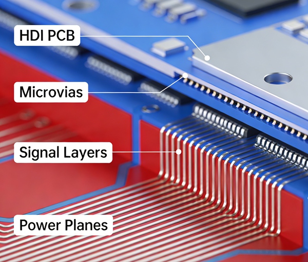
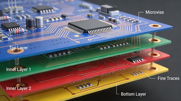
HDI PCB manufacturing involves advanced fabrication processes such as laser drilling, sequential lamination, and fine-line imaging. These processes enable high-density interconnects but also introduce yield and reliability challenges.
This article explains the HDI PCB manufacturing process and yield optimization, helping designers understand how manufacturing constraints influence design decisions and production outcomes.
🔗 Part of the HDI PCB Design Series
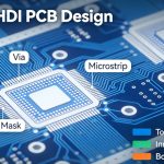
HDI PCB Design: Technology, Stackup, Routing, and Manufacturing
Why HDI PCB Yield Is Challenging
Compared to standard PCBs, HDI boards face:
- Tighter registration tolerances
- Increased lamination cycles
- Microvia plating sensitivity
- Fine-line imaging limitations
Small deviations can cause significant yield loss.
Key Steps in HDI PCB Manufacturing
Laser Drilling of Microvias
- Requires precise depth control
- Influenced by material type and copper thickness
- Poor control leads to incomplete or damaged vias
Sequential Lamination
Each lamination cycle:
- Adds complexity
- Increases cost
- Raises risk of misregistration
Minimizing lamination cycles improves yield.
Via Filling and Planarization
Via-in-pad structures require:
- Copper filling
- Surface planarization
Improper filling causes solder voids and reliability failures.
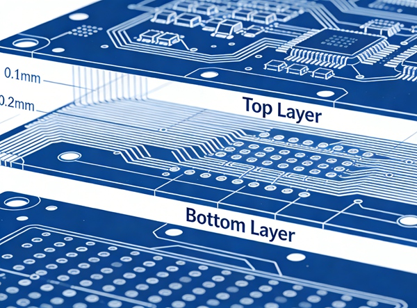
Fine-Line Imaging and Etching
HDI designs use:
- Narrow trace widths
- Tight spacing
Etching uniformity and process stability are critical for yield.
Material Selection and Process Compatibility
Manufacturing yield depends on:
- Laser drillability
- Resin flow behavior
- Thermal expansion characteristics
Materials must be compatible across all HDI processes.
Design Choices That Affect Yield
Designers should avoid:
- Excessive stacked microvias
- Aggressive minimum trace rules everywhere
- Overly complex stackups
Yield-friendly design improves cost and lead time.
🔗 Design influences:
HDI PCB Stackup Design Strategies
HDI PCB Routing Rules and BGA Fanout Techniques
Quality Control and Inspection
Common inspection methods:
- AOI
- X-ray inspection
- Cross-section analysis
Inspection focuses heavily on microvia integrity.
Yield Optimization Strategies
To improve HDI yield:
- Choose the simplest viable stackup
- Limit microvia stacking
- Align routing rules with fab capability
- Engage manufacturers early for DFM reviews
Pilot Builds and Process Validation
Before mass production:
- Run pilot builds
- Analyze yield data
- Adjust design or process parameters
Early validation reduces large-scale failures.
Conclusion
HDI PCB manufacturing success depends on close coordination between design and fabrication. By understanding HDI processes and designing for yield, engineers can achieve reliable, scalable, and cost-effective production.
This article establishes the manufacturing authority layer of the HDI PCB Design cluster.
FAQ – HDI PCB Manufacturing & Yield
A: Advanced processes and tighter tolerances increase sensitivity to variation.
A: Most designs limit to 1–2 sequential laminations for yield and cost control.
A: Yes. They require precise alignment and high-quality via filling.
A: No. Most yield issues originate from design decisions.
A: During stackup and routing planning stages.
A: Yes, but proper planning minimizes delays.