In HDI manufacturing, “yield” is synonymous with “profitability.” With some designs requiring four or more sequential lamination cycles (4+N+4), a 1% loss at each stage can compound into a devastating scrap rate by the final assembly.
Achieving high-yield HDI-PCB production requires more than advanced machinery; it requires a deep understanding of how materials behave under extreme thermal and chemical stress. At Hansphere, we’ve refined our process to tackle these specific failure modes.
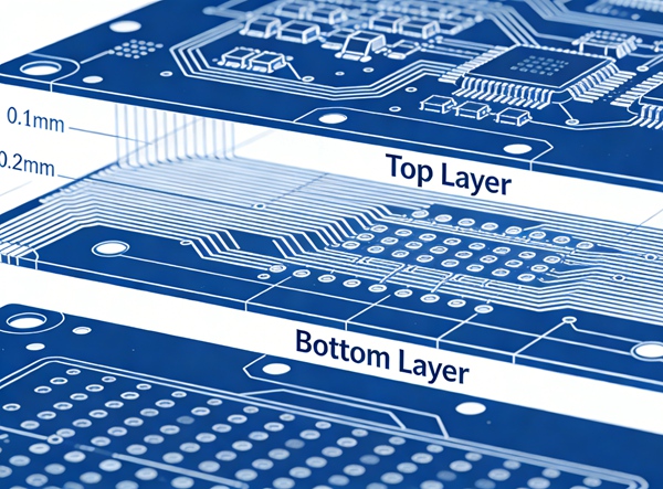
1. The Achilles’ Heel: Dimensional Stability and Registration
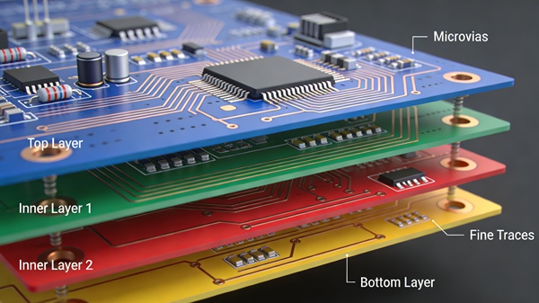
The biggest challenge in HDI is Registration—aligning the laser-drilled microvia to the target pad on the layer below. As layers are added and pressed, the core shrinks and shifts.
- Non-Linear Scaling: We don’t use a fixed scaling factor. We use real-time data from previous batches to apply non-linear compensation to the artwork, anticipating how the specific laminate (like Megtron or Isola) will move.
- LDI (Laser Direct Imaging): By using LDI instead of traditional film, we can adjust the imaging pattern in real-time to match the actual position of the copper features on the panel.
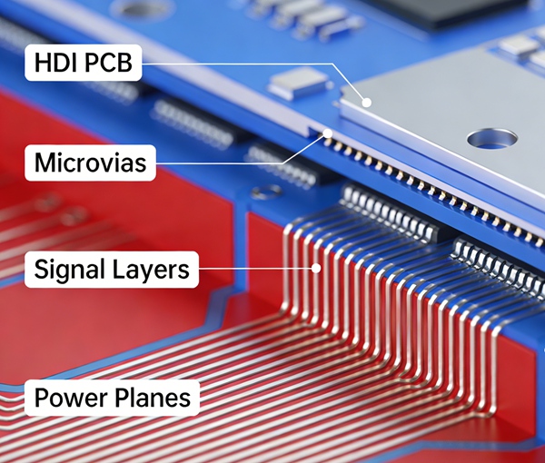
2. Ensuring Microvia Reliability: Filling and Plating
A microvia is only as good as its copper fill. Incomplete filling leads to air bubbles, which expand during PCB Assembly, causing the pad to “lift” or the solder joint to fail.
The VIPPO Standard:
We employ Via-In-Pad Plated Over (VIPPO) technology. After laser drilling, the microvias are electroplated with specialized copper chemistries to ensure a solid, void-free connection.
- Aspect Ratio Control: We strictly maintain an aspect ratio of $\le 0.8:1$ for microvias to ensure the plating solution can circulate effectively to the bottom of the hole.
- Cross-Section Analysis: Every batch at Hansphere undergoes micro-sectioning to verify the grain structure of the plated copper.
5 Steps to Optimize Your HDI Design for Yield
Target: Design Engineers & Quality Assurance Managers
Focus: Reducing Manufacturing Friction
- Step 1: Optimize the Via-to-Pad Ratio
While you can design a 4-mil via in a 6-mil pad, increasing the pad size to 8-mil (if space allows) significantly increases the “registration window,” directly boosting the factory yield and lowering your PCB Manufacturing cost.
- Step 2: Select Compatible Materials
Ensure your Prepreg and Core have compatible Coefficient of Thermal Expansion (CTE) values. Using mismatched materials in a Rigid PCB buildup leads to internal delamination during reflow.
- Step 3: Implement Teardrops on All Microvias
Even in HDI, teardrops are vital. They provide extra copper at the via-to-trace junction, preventing “breakout” if the registration shifts slightly during lamination.
- Step 4: Avoid Stacked Vias if Staggered is Possible
Stacked vias (vias directly on top of vias) are the most difficult to manufacture. If your PCB Design can accommodate Staggered Vias, the mechanical stress on the copper is reduced, improving long-term reliability.
- Step 5: Specify Copper-Filled Vias Early
Don’t wait for the fab house to ask. Explicitly specify copper-filled microvias in your fab notes to ensure the board surface is perfectly flat for fine-pitch BGA assembly.
3. The Impact of Handling and Cleanliness
In the world of 3-mil traces, a single speck of dust is a “killer defect.”
- Class 10,000 Cleanrooms: Our HDI imaging and lamination areas are strictly controlled to prevent foreign object debris (FOD).
- Automated Optical Inspection (AOI): We use high-resolution AOI after every etching step to catch and repair shorts or opens before the next layer is laminated.
FAQ – HDI PCB Manufacturing & Yield
A: Advanced processes and tighter tolerances increase sensitivity to variation.
A: Most designs limit to 1–2 sequential laminations for yield and cost control.
A: The cost is driven by the number of Lamination Cycles. Each HDI “step” (like 1+N+1) requires the board to go back through the entire process: lamination, drilling, plating, and imaging.
A: Pink ring occurs when the oxide coating is dissolved during the de-smear process. At Hansphere, we use a specialized “Alternative Oxide” treatment that provides superior bond strength and eliminates pink ring issues in High Frequency PCBs.
A: Yes. This is known as Rigid-Flex HDI. It is commonly used in smartphones and medical implants. You can see examples of our work on the Rigid-Flex PCB service page.
A: Yes, but proper planning minimizes delays.
Conclusion
High-yield HDI manufacturing is a delicate dance between chemistry, physics, and mechanical precision. By understanding the constraints of registration and plating, and by partnering with a manufacturer that prioritizes DFM, you can bring even the most complex designs to market with confidence.
Facing Yield Issues with Your Current Supplier? Hansphere’s engineering team specializes in troubleshooting and optimizing complex HDI buildups. Send Us Your Design for a Yield Review or learn more about our quality standards on our About Page.