HDI PCB routing focuses on efficiently escaping fine-pitch components while maintaining signal integrity and manufacturability. Compared to standard PCBs, HDI routing requires tighter design rules, disciplined via usage, and optimized fanout strategies.
This article explains HDI PCB routing rules and BGA fanout techniques, helping engineers maximize routing density without compromising reliability.
🔗 Part of the HDI PCB Design Series
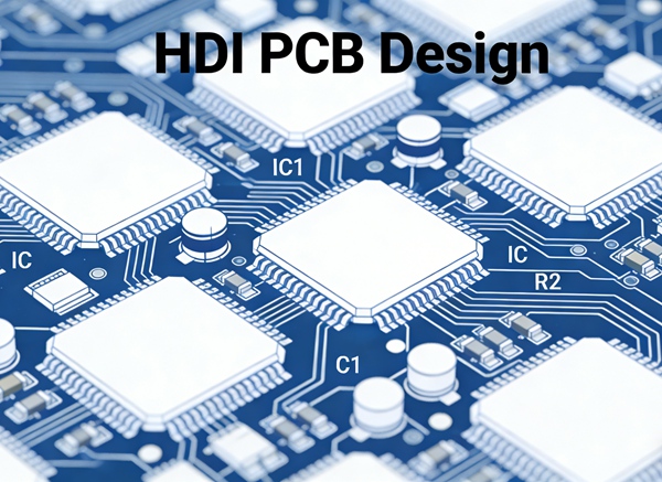
HDI PCB Design: Technology, Stackup, Routing, and Manufacturing
Why Routing Is Different in HDI PCBs
HDI routing must address:
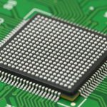
- Fine-pitch BGAs
- Limited surface routing space
- Microvia placement constraints
- Impedance control at small geometries
Routing success depends on stackup and via planning.
🔗 Stackup foundation:
HDI PCB Stackup Design Strategies
BGA Fanout Strategies in HDI Design
Dogbone Fanout (Limited Use)
- Uses short traces to vias
- Works for larger BGA pitches
- Quickly consumes routing space
Not suitable for fine-pitch HDI BGAs.
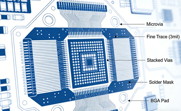
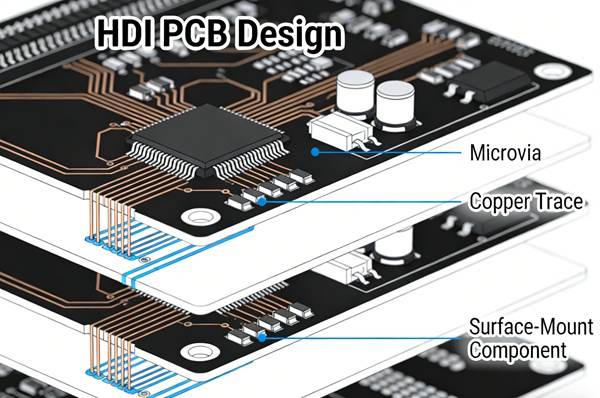
Via-in-Pad Fanout
- Microvias placed directly in pads
- Enables dense routing
- Requires via filling and planarization
Essential for pitches ≤ 0.8 mm.
Microvia-in-Pad with Sequential Fanout
- Escapes signals layer by layer
- Supports ultra-fine-pitch BGAs
- Requires precise stackup planning
HDI Routing Rules and Best Practices
Trace Width and Spacing
- Follow fabricator minimums
- Use consistent geometries
- Avoid aggressive reductions unless necessary
Fine lines increase yield risk.
Via Placement and Transitions
Best practices:
- Minimize via count
- Avoid unnecessary layer transitions
- Use staggered microvias
🔗 Via rules:
Microvias, Blind and Buried Vias in HDI PCB Design
Differential Pair Routing
Recommendations:
- Maintain pair symmetry
- Minimize skew across vias
- Avoid splitting pairs across different via structures
Short via stubs improve high-speed performance.
Power and Ground Routing in HDI
HDI boards often use:
- Thin power-ground spacing
- Localized decoupling near BGAs
- Microvias for power delivery
Proper power routing improves signal integrity.
Avoiding Common Routing Mistakes
Common errors include:
- Overusing stacked microvias
- Excessive layer transitions
- Ignoring return path continuity
These mistakes increase both cost and failure risk.
Routing Density vs Manufacturability
High density must be balanced with yield.
Guidelines:
- Choose conservative rules where possible
- Validate with fabricator capabilities
- Avoid pushing all areas to minimum limits
Best Practices Summary
To route HDI PCBs effectively:
- Select appropriate fanout strategy early
- Use via-in-pad where density demands
- Minimize via transitions
- Maintain impedance and return paths
- Balance density with yield
Conclusion
HDI PCB routing and fanout techniques are essential for unlocking the benefits of high-density interconnect technology. With disciplined routing rules and careful via planning, engineers can achieve compact, reliable, and manufacturable HDI designs.
This article completes the routing execution layer of the HDI PCB Design cluster.
FAQ – HDI PCB Routing & Fanout
A: When BGA pitch is ≤ 0.8 mm or routing space is severely limited.
A: Only for larger pitch components or non-critical areas.
A: Depends on BGA pitch and signal count; HDI often reduces total layer count.
A: Yes. Shorter vias and optimized routing paths reduce parasitics.
A: Yes. It reduces yield and increases cost.
A: No. Stackup and routing must be planned together.