HDI PCB stackup design defines the electrical performance, routing density, manufacturability, and reliability of the entire board. Unlike conventional PCBs, HDI stackups must be designed around microvias, sequential lamination, and fine-pitch component requirements.
This article explains HDI PCB stackup design strategies, covering layer buildup methods, via structures, impedance control, and practical design trade-offs.
🔗 Part of the HDI PCB Design Series
HDI PCB Design: Technology, Stackup, Routing, and Manufacturing
Why Stackup Design Is Critical in HDI PCBs
In HDI designs, stackup decisions directly affect:
- Microvia feasibility
- Routing efficiency
- Signal integrity
- Fabrication yield
- Cost and lead time
A poor stackup cannot be fixed at the routing stage.
Common HDI Stackup Structures
1+N+1 HDI Stackup
- One HDI buildup layer on each side
- Microvias connect outer layers to adjacent inner layers
- Simplest and most cost-effective HDI structure
Often used for moderate-density designs.
2+N+2 and Higher-Order Stackups
- Multiple sequential buildup layers
- Supports very fine-pitch BGAs
- Higher cost and yield risk
Used in smartphones and advanced computing systems.
Sequential Lamination and Layer Buildup
HDI PCBs are built in stages:
- Core fabrication
- Microvia drilling and plating
- Buildup lamination
- Repetition for additional layers
Each lamination cycle increases complexity and cost.
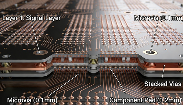
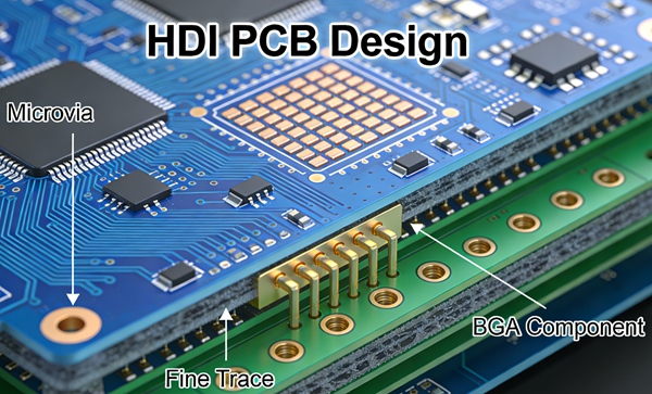
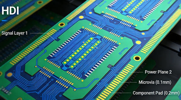
Microvia Placement Within the Stackup
Best practices:
- Keep microvias shallow (1 layer)
- Avoid excessive stacking
- Prefer staggered microvia structures
🔗 Via design foundation:
Microvias, Blind and Buried Vias in HDI PCB Design
Impedance Control in HDI Stackups
Fine trace geometries require precise dielectric control.
Key considerations:
- Thin dielectric layers improve impedance accuracy
- Copper thickness control is critical
- Stackup symmetry reduces warpage
Early impedance modeling is essential.
Power and Ground Distribution
HDI stackups often include:
- Dedicated power and ground layers
- Thin dielectric spacing for low impedance
- Short return paths
Proper power integrity planning improves signal quality.
Material Selection for HDI Stackups
Material choices affect:
- Laser drillability
- Thermal reliability
- Loss characteristics
Low-loss materials may be required for high-speed HDI designs.
Mechanical and Reliability Considerations
HDI stackups must withstand:
- Thermal cycling
- Assembly stress
- Long-term operation
Common risks include:
- Microvia cracking
- Delamination
- Warpage
Stackup symmetry and conservative via structures mitigate these risks.
Cost vs Performance Trade-offs
Designers must balance:
- Layer count
- Buildup complexity
- Manufacturing yield
Not all designs require multi-stage HDI stackups.
Best Practices Summary
To design effective HDI PCB stackups:
- Select the simplest stackup that meets routing needs
- Minimize sequential lamination cycles
- Use staggered microvias
- Control impedance through precise dielectric planning
- Collaborate with fabricators early
Conclusion
HDI PCB stackup design is the structural foundation of high-density interconnect boards. Thoughtful planning of layer buildup, microvia structures, and materials enables reliable, manufacturable, and cost-effective HDI designs.
This article establishes the architectural backbone of the HDI PCB Design content cluster.
FAQ – HDI PCB Stackup Design
A: 1+N+1 is the most widely used due to its balance of density and cost.
A: Most designs use 1–2 buildup layers; more layers increase risk and cost.
A: Yes. Short microvias and controlled impedance layers improve signal performance.
A: Yes. Symmetric stackups reduce warpage and improve reliability.
A: For high-speed and high-frequency applications where signal loss is critical.
A: In some cases, yes—by improving routing efficiency.