Choosing between HDI PCB and standard PCB technology is a critical design decision that affects cost, performance, reliability, and manufacturability. While HDI offers higher routing density and better electrical performance, it also introduces higher fabrication complexity and cost.
This article compares HDI PCB vs standard PCB, helping engineers and decision-makers evaluate the trade-offs and determine the most suitable solution.
🔗 Part of the HDI PCB Design Series
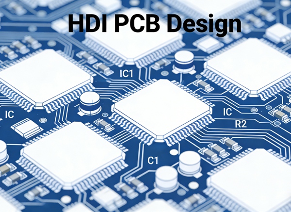
HDI PCB Design: Technology, Stackup, Routing, and Manufacturing
What Makes HDI PCBs More Complex?
HDI PCB complexity comes from:
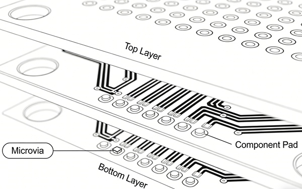
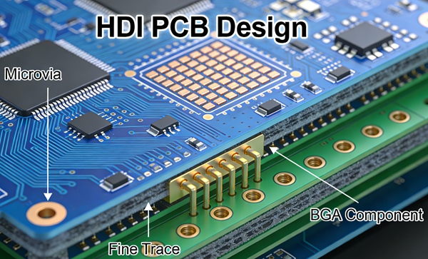
- Microvias and laser drilling
- Sequential lamination
- Fine-line imaging
- Tight registration tolerances
Each adds cost and yield risk compared to standard PCBs.
Cost Comparison: HDI vs Standard PCB
Where HDI Costs More
- Advanced materials
- Multiple lamination cycles
- Via filling and planarization
- Longer lead times
Where HDI Can Reduce System Cost
- Smaller board size
- Fewer layers in some cases
- Reduced connectors and assembly steps
Total system cost—not PCB price alone—should be evaluated.
Design Trade-offs
Routing Density vs Manufacturability
- HDI enables fine-pitch BGA fanout
- Aggressive density increases yield risk
Designers must balance density and producibility.
Electrical Performance
HDI benefits include:
- Shorter via stubs
- Improved signal integrity
- Better high-speed performance
Reliability Considerations
Potential risks:
- Microvia cracking
- Delamination
- Higher sensitivity to process variation
Conservative design mitigates these risks.
When HDI PCB Is the Right Choice
HDI is recommended when:
- BGA pitch ≤ 0.8 mm
- Board size is constrained
- High-speed signals dominate
- System integration benefits justify cost
When Standard PCB Is Enough
Standard PCB designs remain suitable when:
- Component pitch is moderate
- Routing density is manageable
- Cost pressure is high
- Volume is low to medium
Decision-Making Checklist
Before choosing HDI, ask:
- Is HDI required for routing feasibility?
- Are fabricators capable of consistent HDI yield?
- Does system-level cost benefit justify HDI?
- Can risks be mitigated through design discipline?
Best Practices Summary
- Do not choose HDI by default
- Evaluate total system cost
- Involve manufacturers early
- Use the simplest HDI structure possible
Conclusion
HDI PCB technology offers powerful advantages but comes with added complexity and cost. A disciplined evaluation of design requirements, manufacturability, and system-level benefits is essential to determine whether HDI is the right choice.
This article provides the decision framework for the HDI PCB Design content cluster.
FAQ – HDI vs Standard PCB
A: Per-board cost is higher, but total system cost may be lower.
A: Yes, in some designs HDI improves routing efficiency enough to reduce layers.
A: Not inherently. Reliability depends on design and manufacturing quality.
A: Only if routing or performance requirements demand it.
A: Typically yes, due to additional fabrication steps.
A: Usually no, due to fundamental via and routing differences.