In the era of IoT, AI servers, and 5G telecommunications, “High-Speed” is no longer a niche category—it is the standard. When signal switching speeds reach the nanosecond range, PCB traces stop acting like simple conductors and begin behaving like transmission lines.
At Hansphere, we understand that high-speed PCB design is a balance of geometry, material science, and electromagnetic theory. Here is our expert guide to navigating these complexities.
1. What Defines a “High-Speed” Design?
It’s a common misconception that high-speed is defined by the clock frequency. In reality, it is defined by the rise time (or fall time) of the signal. If the physical length of the trace is significant compared to the signal’s rise time, you are in the high-speed domain.
- The Threshold: When the trace length > 1/6th of the signal’s electrical wavelength, transmission line effects like reflections and ringing become dominant.
- Key Challenges: Signal attenuation, propagation delay, and Electromagnetic Interference (EMI).
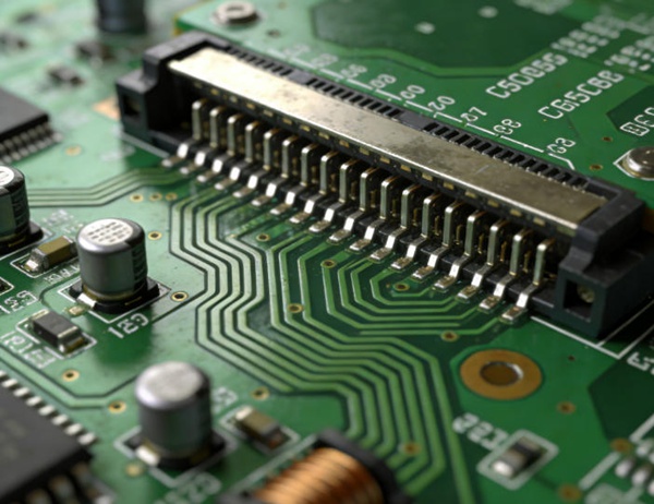
2. Critical Design Pillars for Signal Integrity (SI)
Controlled Impedance (Zo)
To prevent signal reflections, the impedance of the trace must match the source and load. Any “discontinuity”—such as a poorly designed via or a change in trace width—will cause the signal to bounce back, corrupting data.
- Hansphere Tip: We utilize advanced TDR (Time Domain Reflectometry) testing during PCB Manufacturing to verify that your board meets the specified $\pm5\%$ or $\pm10\%$ impedance tolerance.
Crosstalk Mitigation
Crosstalk occurs when energy from one trace “leaks” into an adjacent one through capacitive or inductive coupling.
- The 3W Rule: Maintain a spacing of at least three times the trace width between parallel high-speed lines.
- Orthogonal Routing: When routing on adjacent layers, ensure traces run perpendicular to each other to minimize the coupling area.
Power Integrity (PI) & Decoupling
High-speed ICs require massive amounts of instantaneous current. Without a robust Power Delivery Network (PDN), your signals will suffer from “Ground Bounce” and “VCC Sag.”
- Strategy: Use low-ESR decoupling capacitors placed as close as possible to the IC power pins. For multi-layer Rigid PCBs, utilize plane capacitance by placing power and ground layers close together.
5 Steps to Execute a High-Speed PCB Project
Target: System Architects & Senior Layout Engineers
Goal: First-Pass Success in Complex Designs
- Step 1: Pre-Layout Material Selection
Standard FR-4 has a high Dissipation Factor (Df), which can “eat” your signal at high frequencies. For 10GHz+ designs, consider high-speed laminates like Rogers, Isola, or Panasonic Megtron 6.
Related: See our guide on Ceramic PCBs for extreme thermal and frequency requirements - Step 2: Define a Symmetric Stack-up
A balanced stack-up prevents board warping during PCB Assembly and provides a consistent reference for high-speed signals.
- Step 3: Implement Differential Pair Tuning
Ensure that differential pairs (like those in PCIe or USB-C) are length-matched to within 5 mils. This ensures the signals arrive at the receiver at the exact same time, maintaining the “differential” nature of the link.
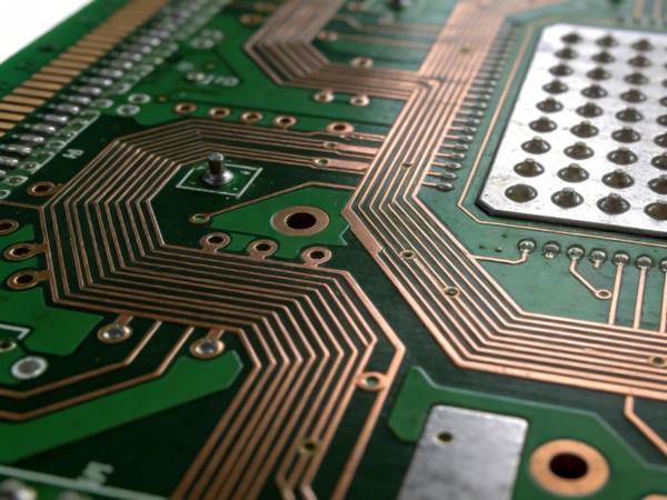
- Step 4: Manage Via Transitions
Every time a signal changes layers through a via, it encounters an impedance change.
Stitching Vias: Place a ground via immediately next to a signal via to provide a continuous return path for the current.
HDI Advantage: Use HDI-PCB technology with microvias to reduce parasitic inductance. - Step 5: Post-Layout Verification
Perform a full DRC (Design Rule Check) and, if budget allows, an EMI scan or Signal Integrity simulation to catch “hot spots” before fabrication.
3. Advanced Trends in High-Speed Boards
Embedded Components: Placing resistors or capacitors inside the PCB layers to shorten the signal path even further.
Flexible High-Speed Interconnects: Combining high-speed signals with Flex-PCB or Rigid-Flex PCB technology for space-constrained aerospace and medical applications.
High-Speed Design FAQ
A: At high speeds, current follows the path of least inductance, not least resistance. This path is usually directly underneath the trace on the reference plane. If you break that plane, the current will “loop” around the break, creating a massive EMI antenna.
A: When your signal speeds exceed 5Gbps or your component pitch (like BGA) is less than 0.8mm. Microvias significantly reduce the “stub” effect that causes signal reflections.
A: Yes. We offer a complimentary DFM and stack-up review for all PCB Design projects to ensure the materials selected match your impedance requirements and budget.
Conclusion
High-speed PCB design is where electronics meet physics. By focusing on impedance control, return path continuity, and proper material selection, you can build reliable, high-performance systems that pass EMI testing on the first try.
Ready to start your next high-speed project? Hansphere’s engineering team is ready to assist with high-tier fabrication and precision assembly. Get an Instant Quote or Explore Our About Page to see our advanced capabilities.